SNVS294S November 2004 – May 2016 LM3671 , LM3671-Q1
PRODUCTION DATA.
- 1 Features
- 2 Applications
- 3 Description
- 4 Revision History
- 5 Pin Configuration and Functions
- 6 Specifications
- 7 Detailed Description
- 8 Application and Implementation
- 9 Power Supply Recommendations
- 10Layout
- 11Device and Documentation Support
- 12Mechanical, Packaging, and Orderable Information
Package Options
Mechanical Data (Package|Pins)
Thermal pad, mechanical data (Package|Pins)
Orderable Information
8 Application and Implementation
NOTE
Information in the following applications sections is not part of the TI component specification, and TI does not warrant its accuracy or completeness. TI’s customers are responsible for determining suitability of components for their purposes. Customers should validate and test their design implementation to confirm system functionality.
8.1 Application Information
The external control of this device is very easy. First make sure the correct voltage been applied at VIN pin, then simply apply the voltage at EN pin according to the Electrical Characteristics to enable or disable the output voltage.
8.2 Typical Application
8.2.1 Typical Application: Fixed-Voltage Version
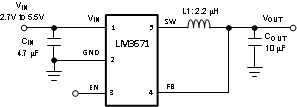 Figure 32. LM3671 Fixed-Voltage Typical Application Circuit
8.2.1.1 Design Requirements
Two ceramic capacitors and one inductor required for this application. These three external components need to be selected very carefully for property operation. Please read Detailed Design Procedure.
8.2.1.2 Detailed Design Procedure
8.2.1.2.1 Inductor Selection
There are two main considerations when choosing an inductor; the inductor should not saturate, and the inductor current ripple should be small enough to achieve the desired output voltage ripple. Different saturation current rating specifications are followed by different manufacturers so attention must be given to details. Saturation current ratings are typically specified at 25°C. However, ratings at the maximum ambient temperature of application should be requested from the manufacturer. The minimum value of inductance to specify good performance is 1.76 µH at ILIM (typical) DC current over the ambient temperature range. Shielded inductors radiate less noise and should be preferred.
There are two methods to choose the inductor saturation current rating.
8.2.1.2.1.1 Method 1
The saturation current should be greater than the sum of the maximum load current and the worst case average to peak inductor current. This can be written as

where
- IRIPPLE: average to peak inductor current
- IOUTMAX: maximum load current (600 mA)
- VIN: maximum input voltage in application
- L : min inductor value including worst case tolerances (30% drop can be considered for method 1)
- f : minimum switching frequency (1.6 MHz)
- VOUT: output voltage
8.2.1.2.1.2 Method 2
A more conservative and recommended approach is to choose an inductor that has a saturation current rating greater than the maximum current limit of 1150 mA.
A 2.2-µH inductor with a saturation current rating of at least 1150 mA is recommended for most applications. Inductor resistance should be less than 0.3 Ω for good efficiency. Table 1 lists suggested inductors and suppliers. For low-cost applications, an unshielded bobbin inductor could be considered. For noise critical applications, a toroidal or shielded-bobbin inductor should be used. A good practice is to lay out the board with overlapping footprints of both types for design flexibility. This allows substitution of a low-noise shielded inductor, in the event that noise from low-cost bobbin models is unacceptable.
8.2.1.2.2 Input Capacitor Selection
A ceramic input capacitor of 4.7 µF, 6.3 V is sufficient for most applications. Place the input capacitor as close as possible to the VIN pin of the device. A larger value may be used for improved input voltage filtering. Use X7R or X5R types; do not use Y5V. DC bias characteristics of ceramic capacitors must be considered when selecting case sizes like 0805 and 0603. The minimum input capacitance to specify good performance is 2.2 µF at 3-V DC bias; 1.5 µF at 5-V DC bias including tolerances and over ambient temperature range. The input filter capacitor supplies current to the PFET switch of the LM3671 in the first half of each cycle and reduces voltage ripple imposed on the input power source. A ceramic capacitor’s low ESR provides the best noise filtering of the input voltage spikes due to this rapidly changing current. Select a capacitor with sufficient ripple current rating. The input current ripple can be calculated as:
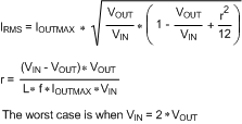
Table 1. Suggested Inductors and Their Suppliers
| MODEL | VENDOR | DIMENSIONS L × W × H (mm) | D.C.R (maximum)(mΩ) |
|---|---|---|---|
| DO3314-222MX | Coilcraft | 3.3 × 3.3 × 1.4 | 200 |
| LPO3310-222MX | Coilcraft | 3.3 × 3.3 × 1 | 150 |
| ELL5GM2R2N | Panasonic | 5.2 × 5.2 × 1.5 | 53 |
| CDRH2D14NP-2R2NC | Sumida | 3.2 × 3.2 × 1.55 | 94 |
8.2.1.2.3 Output Capacitor Selection
A ceramic output capacitor of 10 µF, 6.3 V is sufficient for most applications. Use X7R or X5R types; do not use Y5V. DC bias characteristics of ceramic capacitors must be considered when selecting case sizes like 0805 and 0603. DC bias characteristics vary from manufacturer to manufacturer and dc bias curves should be requested from them as part of the capacitor selection process.
The minimum output capacitance to specify good performance is 5.75 µF at 1.8-V DC bias including tolerances and over ambient temperature range. The output filter capacitor smoothes out current flow from the inductor to the load, helps maintain a steady output voltage during transient load changes and reduces output voltage ripple. These capacitors must be selected with sufficient capacitance and sufficiently low ESR to perform these functions.
The output voltage ripple is caused by the charging and discharging of the output capacitor and by the RESR and can be calculated as:
Voltage peak-to-peak ripple due to capacitance can be expressed by Equation 4:

Voltage peak-to-peak ripple due to ESR can be expressed by Equation 5:
Because these two components are out of phase the rms (root mean squared) value can be used to get an approximate value of peak-to-peak ripple.
The peak-to-peak ripple voltage, rms value can be expressed by Equation 6:

Note that the output voltage ripple is dependent on the inductor current ripple and the equivalent series resistance of the output capacitor (RESR).
The RESR is frequency dependent (as well as temperature dependent); make sure the value used for calculations is at the switching frequency of the part.
Table 2. Suggested Capacitors and Their Suppliers
| MODEL | TYPE | VENDOR | VOLTAGE RATING (V) | CASE SIZE INCH (mm) |
|---|---|---|---|---|
| 4.7 µF for CIN | ||||
| C2012X5R0J475K | Ceramic, X5R | TDK | 6.3 | 0805 (2012) |
| JMK212BJ475K | Ceramic, X5R | Taiyo-Yuden | 6.3 | 0805 (2012) |
| GRM21BR60J475K | Ceramic, X5R | Murata | 6.3 | 0805 (2012) |
| C1608X5R0J475K | Ceramic, X5R | TDK | 6.3 | 0603 (1608) |
| 10 µF for COUT | ||||
| GRM21BR60J106K | Ceramic, X5R | Murata | 6.3 | 0805 (2012) |
| JMK212BJ106K | Ceramic, X5R | Taiyo-Yuden | 6.3 | 0805 (2012) |
| C2012X5R0J106K | Ceramic, X5R | TDK | 6.3 | 0805 (2012) |
| C1608X5R0J106K | Ceramic, X5R | TDK | 6.3 | 0603 (1608) |
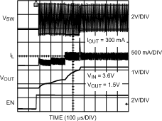
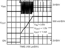
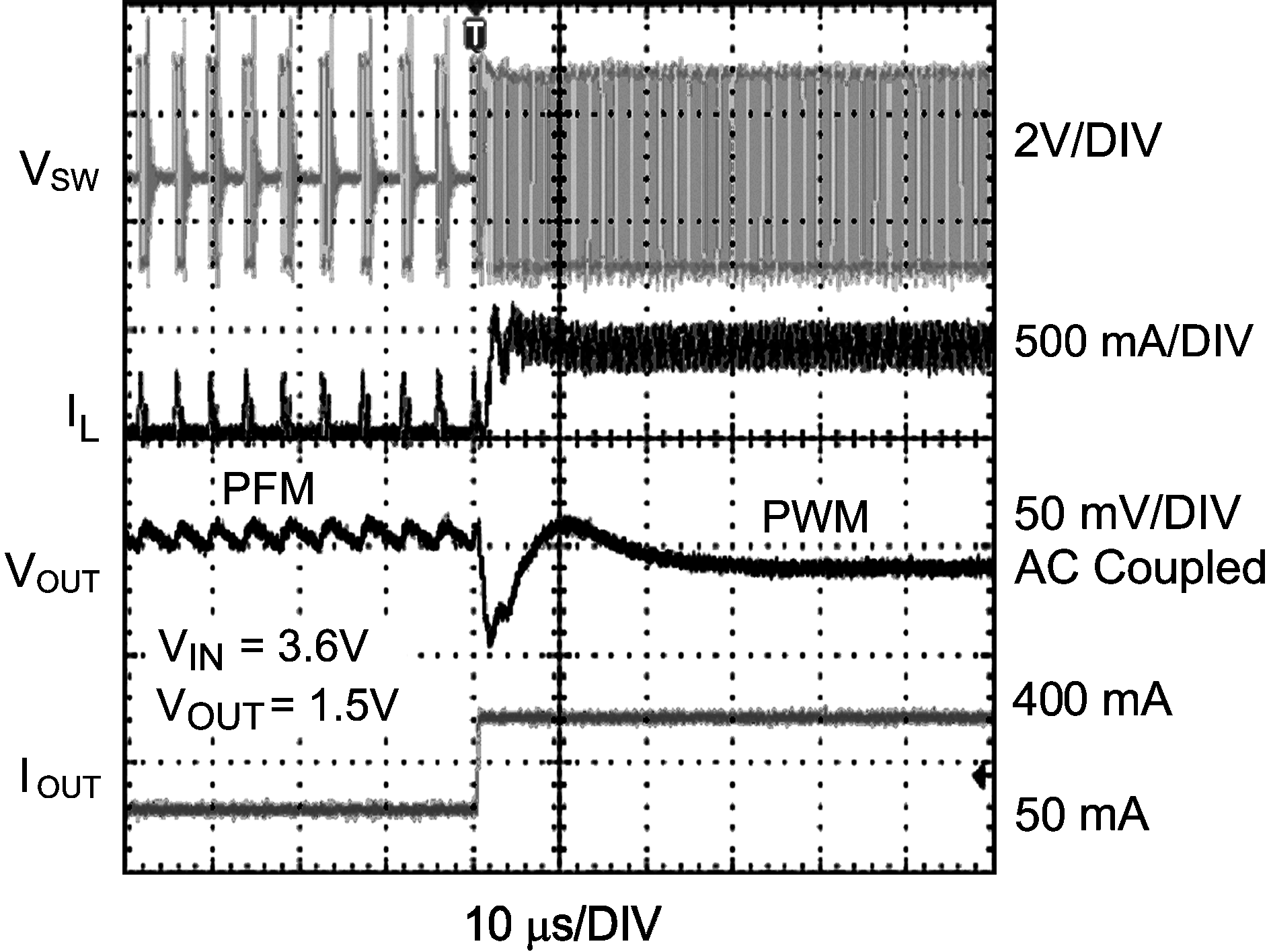
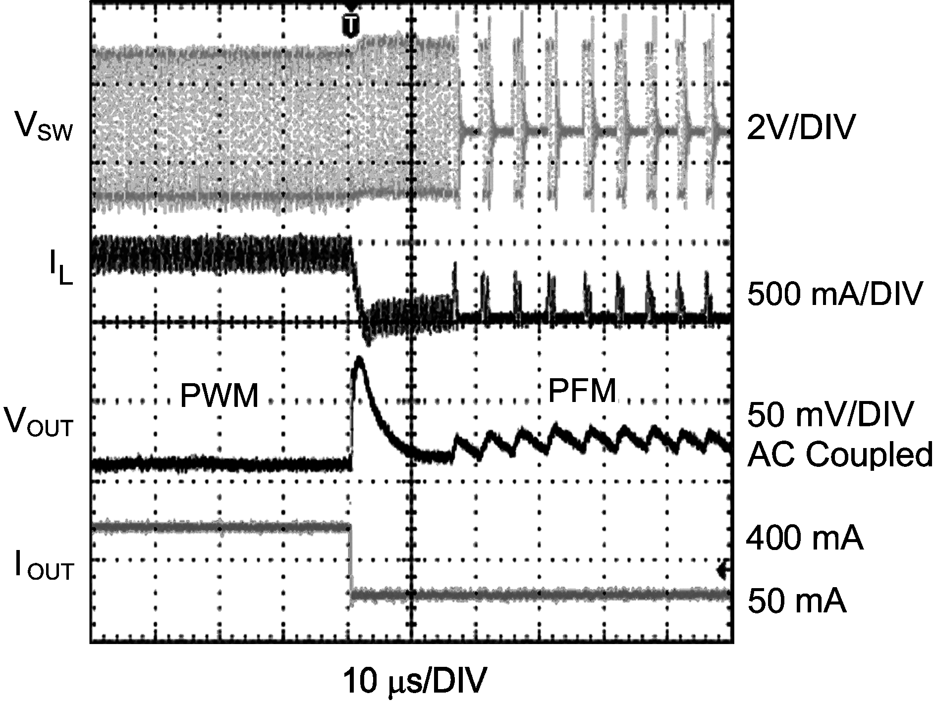
8.2.1.3 Application Curves
8.2.2 Typical Application: ADJ Version
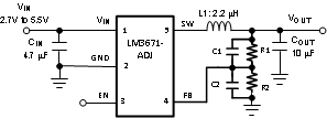 Figure 35. Typical Application Circuit for ADJ Version
8.2.2.1 Design Requirements
| DESIGN PARAMETER | EXAMPLE VALUE |
|---|---|
| Input voltage range | 2.7 V to 5.5 V |
| Input capacitor | 4.7 µF |
| Output capacitor | 10 µF |
| Inductor | 2.2 µH |
| ADJ programmable output voltage | 1.1 V to 3.3 V |
8.2.2.2 Detailed Design Procedure
8.2.2.2.1 Output Voltage Selection for LM3671-ADJ
The output voltage of the adjustable parts can be programmed through the resistor network connected from VOUT to FB, then to GND. VOUT is adjusted to make the voltage at FB equal to 0.5 V. The resistor from FB to GND (R2) should be 200 kΩ to keep the current drawn through this network well below the 16-µA quiescent current level (PFM mode) but large enough that it is not susceptible to noise. If R2 is 200 kΩ, and VFB is 0.5 V, the current through the resistor feedback network will be 2.5 µA. The output voltage of the adjustable parts ranges from 1.1 V to 3.3 V.
The formula for output voltage selection is:

where
- VOUT: output voltage (volts)
- VFB : feedback voltage = 0.5 V
- R1: feedback resistor from VOUT to FB
- R2: feedback resistor from FB to GND
For any output voltage greater than or equal to 1.1 V, a zero must be added around 45 kHz for stability. The formula for calculation of C1 is:

For output voltages higher than 2.5 V, a pole must be placed at 45 kHz as well. If the pole and zero are at the same frequency the formula for calculation of C2 is:

The formula for location of zero and pole frequency created by adding C1 and C2 is given below. By adding C1, a zero as well as a higher frequency pole is introduced.


See the Table 3 table.
Table 3. LM3671-ADJ Configurations for Various VOUT
(Circuit of Figure 35)
| VOUT (V) | R1 (kΩ) | R2 (kΩ) | C1 (pF) | C2 (pF) | L (µH) | CIN (µF) | COUT (µF) |
|---|---|---|---|---|---|---|---|
| 0.9 | 160 | 200 | 22 | none | 2.2 | 4.7 | 10 |
| 1.1 | 240 | 200 | 15 | none | 2.2 | 4.7 | 10 |
| 1.2 | 280 | 200 | 12 | none | 2.2 | 4.7 | 10 |
| 1.3 | 320 | 200 | 12 | none | 2.2 | 4.7 | 10 |
| 1.5 | 357 | 178 | 10 | none | 2.2 | 4.7 | 10 |
| 1.6 | 442 | 200 | 8.2 | none | 2.2 | 4.7 | 10 |
| 1.7 | 432 | 178 | 8.2 | none | 2.2 | 4.7 | 10 |
| 1.8 | 464 | 178 | 8.2 | none | 2.2 | 4.7 | 10 |
| 1.875 | 523 | 191 | 6.8 | none | 2.2 | 4.7 | 10 |
| 2.5 | 402 | 100 | 8.2 | none | 2.2 | 4.7 | 10 |
| 2.8 | 464 | 100 | 8.2 | 33 | 2.2 | 4.7 | 10 |
| 3.3 | 562 | 100 | 6.8 | 33 | 2.2 | 4.7 | 10 |
8.2.2.3 Application Curves
