SNVS555D January 2008 – December 2014 LM3881
PRODUCTION DATA.
- 1 Features
- 2 Applications
- 3 Description
- 4 Revision History
- 5 Pin Configuration and Functions
- 6 Specifications
- 7 Detailed Description
- 8 Application and Implementation
- 9 Power Supply Recommendations
- 10Layout
- 11Device and Documentation Support
- 12Mechanical, Packaging, and Orderable Information
Package Options
Mechanical Data (Package|Pins)
- DGK|8
Thermal pad, mechanical data (Package|Pins)
Orderable Information
6 Specifications
6.1 Absolute Maximum Ratings
over operating free-air temperature (unless otherwise noted) (1)(2)| MIN | MAX | UNIT | ||
|---|---|---|---|---|
| VCC, EN, INV, TADJ, FLAG1, FLAG2, FLAG3 to GND | –0.3 | 6.0 | V | |
| Junction Temperature | 150 | °C | ||
| Lead Temperature (Soldering, 5 s) | 260 | °C |
(1) Stresses beyond those listed under Absolute Maximum Ratings may cause permanent damage to the device. These are stress ratings only, which do not imply functional operation of the device at these or any other conditions beyond those indicated under Recommended Operating Conditions. Exposure to absolute-maximum-rated conditions for extended periods may affect device reliability.
(2) If Military/Aerospace specified devices are required, please contact the Texas Instruments Sales Office/Distributors for availability and specifications.
6.2 Handling Ratings
| MIN | MAX | UNIT | |||
|---|---|---|---|---|---|
| Tstg | Storage temperature range | –65 | 150 | °C | |
| V(ESD) | Electrostatic discharge | Human body model (HBM), per ANSI/ESDA/JEDEC JS-001, all pins(1) | 2 | kV | |
(1) JEDEC document JEP155 states that 500-V HBM allows safe manufacturing with a standard ESD control process.
6.3 Recommended Operating Conditions
over operating free-air temperature range (unless otherwise noted)| MIN | MAX | UNIT | ||
|---|---|---|---|---|
| VCC to GND | 2.7 | 5.5 | V | |
| EN, INV, TADJ, FLAG1, FLAG2, FLAG3 to GND | –0.3 | VCC + 0.3 | V | |
| Junction Temperature | –40 | 125 | °C | |
6.4 Thermal Information
| THERMAL METRIC(1) | LM3881 | UNIT | |
|---|---|---|---|
| DGK | |||
| 8 PINS | |||
| RθJA | Junction-to-ambient thermal resistance | 224.5 | °C/W |
| RθJC(top) | Junction-to-case (top) thermal resistance | 107.6 | |
| RθJB | Junction-to-board thermal resistance | 145.3 | |
| ψJT | Junction-to-top characterization parameter | 31.8 | |
| ψJB | Junction-to-board characterization parameter | 143.7 | |
(1) For more information about traditional and new thermal metrics, see the IC Package Thermal Metrics application report, SPRA953.
6.5 Electrical Characteristics
over operating free-air temperature range (unless otherwise noted). Minimum and Maximum limits are ensured through test, design or statistical correlation. Typical values represent the most likely parametric norm at TJ = 25°C and are provided for reference purposes only. TJ = –40°C to +125°C, VCC = 3.3 V, unless otherwise specified.| PARAMETER | TEST CONDITIONS | MIN(1) | TYP(2) | MAX(1) | UNIT | |
|---|---|---|---|---|---|---|
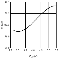
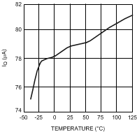
| IQ | Operating Quiescent Current | 80 | 110 | µA | ||
| OPEN-DRAIN FLAGS | ||||||
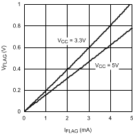
| IFLAG | FLAGx Leakage Current | VFLAGx = 3.3 V | 0.001 | 1 | µA | |
| VOL | FLAGx Output Voltage Low | IFLAGx = 1.2 mA | 0.4 | V | ||
| TIME DELAYS | ||||||
| ITADJ_SRC | TADJ Source Current | 4 | 12 | 20 | µA | |
| ITADJ_SNK | TADJ Sink Current | 4 | 12 | 20 | µA | |
| VHTH | High Threshold Level | 1.0 | 1.22 | 1.4 | V | |
| VLTH | Low Threshold Level | 0.3 | 0.5 | 0.7 | V | |
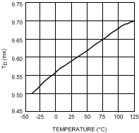
| TCLK | Clock Cycle | CADJ = 10 nF | 1.2 | ms | ||
| TD1, TD4 | Flag Time Delay | 9 | 10 | Clock cycles | ||
| TD2, TD3, TD5, TD6 | Flag Time Delay | 8 | Clock cycles | |||
| ENABLE PIN | ||||||
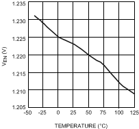
| VEN | EN Pin Threshold | 1.0 | 1.22 | 1.5 | V | |
| IEN | EN Pin Pullup Current | VEN = 0 V | 7 | µA | ||
| INV PIN | ||||||
| VIH_INV | Invert Pin VIH | 90% VCC | V | |||
| VIL_INV | Invert Pin VIL | 10% VCC | V | |||
(1) Limits are 100% production tested at 25°C. Limits over the operating temperature range are ensured through correlation using Statistical Quality Control (SQC) methods. The limits are used to calculate TI's Average Outgoing Quality Level (AOQL).
(2) Typical numbers are at 25°C and represent the most likely parametric norm.
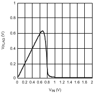
6.6 Typical Characteristics
VCC = 3.3 V unless otherwise specified.