SLCS162 June 2017 LM393-MIL
PRODUCTION DATA.
- 1 Features
- 2 Applications
- 3 Description
- 4 Revision History
- 5 Pin Configuration and Functions
- 6 Specifications
- 7 Detailed Description
- 8 Application and Implementation
- 9 Power Supply Recommendations
- 10Layout
- 11Device and Documentation Support
- 12Mechanical, Packaging, and Orderable Information
Package Options
Mechanical Data (Package|Pins)
- Y|0
Thermal pad, mechanical data (Package|Pins)
Orderable Information
10 Layout
10.1 Layout Guidelines
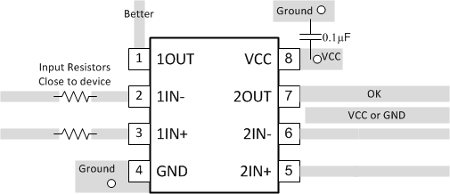
For accurate comparator applications without hysteresis it is important maintain a stable power supply with minimized noise and glitches, which can affect the high level input common-mode voltage range. To achieve this, it is best to add a bypass capacitor between the supply voltage and ground. This should be implemented on the positive power supply and negative supply (if available). If a negative supply is not being used, do not put a capacitor between the IC GND pin and system ground.
10.2 Layout Example
 Figure 10. LM393-MIL Layout Example