SNVS049F February 2000 – March 2016 LM4120
PRODUCTION DATA.
- 1 Features
- 2 Applications
- 3 Description
- 4 Revision History
- 5 Pin Configuration and Functions
- 6 Specifications
- 7 Detailed Description
- 8 Application and Implementation
- 9 Power Supply Recommendations
- 10Layout
- 11Device and Documentation Support
- 12Mechanical, Packaging, and Orderable Information
Package Options
Mechanical Data (Package|Pins)
- DBV|5
Thermal pad, mechanical data (Package|Pins)
Orderable Information
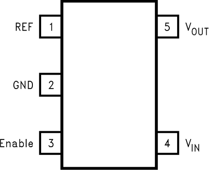
5 Pin Configuration and Functions
DBV Package
5-Pin SOT-23
Top View

Pin Functions
| PIN | I/O | DESCRIPTION | |
|---|---|---|---|
| NAME | NO. | ||
| Enable | 3 | I | Pulled to input for normal operation. Forcing this pin to ground will turn off the output. |
| GND | 2 | — | Negative supply or ground connection |
| REF | 1 | — | REF pin. This pin must be left unconnected. |
| VIN | 4 | I | Positive supply |
| VOUT | 5 | O | Reference output |