SNVSA44B August 2014 – January 2018 LM43601
PRODUCTION DATA.
- 1 Features
- 2 Applications
- 3 Description
- 4 Revision History
- 5 Pin Configuration and Functions
- 6 Specifications
-
7 Detailed Description
- 7.1 Overview
- 7.2 Functional Block Diagram
- 7.3
Feature Description
- 7.3.1 Fixed-Frequency, Peak-Current-Mode Controlled, Step-Down Regulator
- 7.3.2 Light Load Operation
- 7.3.3 Adjustable Output Voltage
- 7.3.4 Enable (ENABLE)
- 7.3.5 VCC, UVLO and BIAS
- 7.3.6 Soft Start and Voltage Tracking (SS/TRK)
- 7.3.7 Switching Frequency (RT) and Synchronization (SYNC)
- 7.3.8 Minimum ON-Time, Minimum OFF-Time, and Frequency Foldback at Dropout Conditions
- 7.3.9 Internal Compensation and CFF
- 7.3.10 Bootstrap Voltage (BOOT)
- 7.3.11 Power Good (PGOOD)
- 7.3.12 Overcurrent and Short-Circuit Protection
- 7.3.13 Thermal Shutdown
- 7.4 Device Functional Modes
-
8 Applications and Implementation
- 8.1 Application Information
- 8.2
Typical Application
- 8.2.1 Design Requirements
- 8.2.2
Detailed Design Procedure
- 8.2.2.1 Custom Design With WEBENCH® Tools
- 8.2.2.2 Output Voltage Setpoint
- 8.2.2.3 Switching Frequency
- 8.2.2.4 Input Capacitors
- 8.2.2.5 Inductor Selection
- 8.2.2.6 Output Capacitor Selection
- 8.2.2.7 Feedforward Capacitor
- 8.2.2.8 Bootstrap Capacitors
- 8.2.2.9 VCC Capacitor
- 8.2.2.10 BIAS Capacitors
- 8.2.2.11 Soft-Start Capacitors
- 8.2.2.12 Undervoltage Lockout Set-Point
- 8.2.2.13 PGOOD
- 8.2.3 Application Curves
- 9 Power Supply Recommendations
- 10Layout
- 11Device and Documentation Support
- 12Mechanical, Packaging, and Orderable Information
Package Options
Mechanical Data (Package|Pins)
- PWP|16
Thermal pad, mechanical data (Package|Pins)
- PWP|16
Orderable Information
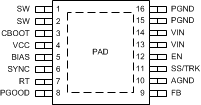
5 Pin Configuration and Functions
PWP Package
16-Pin HTSSOP
Top View

Pin Functions
| PIN | I/O | DESCRIPTION | |
|---|---|---|---|
| NO. | NAME | ||
| 1, 2 | SW | P | Switching output of the regulator. Internally connected to both power MOSFETs. Connect to power inductor. |
| 3 | CBOOT | P | Boot-strap capacitor connection for high-side driver. Connect a high-quality, 470-nF capacitor from CBOOT to SW. |
| 4 | VCC | P | Internal bias supply output for bypassing. Connect bypass capacitor from this pin to AGND. Do not connect external load to this pin. Never short this pin to ground during operation. |
| 5 | BIAS | P | Optional internal LDO supply input. To improve efficiency, TI recommends typing to VOUT when 3.3 V ≤ VOUT ≤ 28 V, or tie to an external 3.3 V or 5 V rail if available. When used, place a bypass capacitor (1 to 10 µF) from this pin to ground. Tie to ground when not in use. Do not float |
| 6 | SYNC | A | Clock input to synchronize switching action to an external clock. Use proper high speed termination to prevent ringing. Connect to ground if not used. Do not float. |
| 7 | RT | A | Connect a resistor RT from this pin to AGND to program switching frequency. Leave floating for 500 kHz default switching frequency. |
| 8 | PGOOD | A | Open drain output for power-good flag. Use a 10-kΩ to 100-kΩ pullup resistor to logic rail or other DC voltage no higher than 12 V. |
| 9 | FB | A | Feedback sense input pin. Connect to the midpoint of feedback divider to set VOUT. Do not short this pin to ground during operation. |
| 10 | AGND | G | Analog ground pin. Ground reference for internal references and logic. Connect to system ground. |
| 11 | SS/TRK | A | Soft-start control pin. Leave floating for internal soft-start slew rate. Connect to a capacitor to extend soft-start time. Connect to external voltage ramp for tracking. |
| 12 | EN | A | Enable input to the LM43601: High = ON and low = OFF. Connect to VIN, or to VIN through resistor divider, or to an external voltage or logic source. Do not float. |
| 13,14 | VIN | P | Supply input pins to internal LDO and high side power FET. Connect to power supply and bypass capacitors CIN. Path from VIN pin to high frequency bypass CIN and PGND must be as short as possible. |
| 15,16 | PGND | G | Power ground pins, connected internally to the low-side power FET. Connect to system ground, PAD, AGND, ground pins of CIN and COUT. Path to CIN must be as short as possible. |
| PAD | G | Low impedance connection to AGND. Connect to PGND on PCB . Major heat dissipation path of the die. Must be used for heat sinking to ground plane on PCB. | |