SNVS397E September 2005 – November 2016 LM5005
PRODUCTION DATA.
- 1 Features
- 2 Applications
- 3 Description
- 4 Revision History
- 5 Pin Configuration and Functions
- 6 Specifications
- 7 Detailed Description
-
8 Application and Implementation
- 8.1 Application Information
- 8.2
Typical Application
- 8.2.1 Design Requirements
- 8.2.2
Detailed Design Procedure
- 8.2.2.1 Frequency Set Resistor (RT)
- 8.2.2.2 Inductor (LF)
- 8.2.2.3 Ramp Capacitor (CRAMP)
- 8.2.2.4 Output Capacitors (COUT)
- 8.2.2.5 Schottky Diode (DF)
- 8.2.2.6 Input Capacitors (CIN)
- 8.2.2.7 VCC Capacitor (CVCC)
- 8.2.2.8 Bootstrap Capacitor (CBST)
- 8.2.2.9 Soft Start Capacitor (CSS)
- 8.2.2.10 Feedback Resistors (RFB1 and RFB2)
- 8.2.2.11 RC Snubber (RS and CS)
- 8.2.2.12 Compensation Components (RC1, CC1, CC2)
- 8.2.2.13 Bill of Materials
- 8.2.3 Application Curves
- 9 Power Supply Recommendations
- 10Layout
- 11Device and Documentation Support
- 12Mechanical, Packaging, and Orderable Information
Package Options
Mechanical Data (Package|Pins)
- PWP|20
Thermal pad, mechanical data (Package|Pins)
- PWP|20
Orderable Information
1 Features
- High-Efficiency DC-DC Buck Converter
- Wide Input Voltage Range From 7 V to 75 V
- Adjustable Output Voltage as Low as 1.225 V
- Output Current as High as 2.5 A
- Junction Temperature Range –40°C to 125°C
- Integrated 75-V, 160-mΩ Buck MOSFET
- Meets EN55022 and CISPR 22 EMI Standards
- ±1.5% Feedback Voltage Accuracy
- Emulated Peak Current-Mode Control
- Ultra-Fast Line and Load Transient Response
- Switching Frequency From 50 kHz to 500 kHz
- Master or Slave Frequency Synchronization Input
- 80-ns Minimum PWM ON Time For Low VOUT
- Monotonic Start-up into Prebiased Output
- Internal High-Voltage VCC Bias Supply Regulator
- Auxiliary Bias Supply Option to VCC
- Configurable Soft Start With Tracking
- Precision Standby and Shutdown Input
- Programmable Input UVLO With Hysteresis
- Remote Shutdown and Standby Control
- Cycle-by-Cycle Overcurrent Protection
- VCC and Gate Drive UVLO Protection
- Thermal Shutdown Protection With Hysteresis
- Thermally-Enhanced 20-Pin HTSSOP Package
2 Applications
- High-Efficiency Point-of-Load Regulators
- Telecommunications Infrastructure
- Factory Automation and Control
SPACER
3 Description
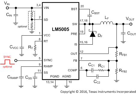
The LM5005 high-voltage buck converter features all of the functions necessary to implement an efficient high-voltage switching regulator with a minimum number of external components. This easy-to-use converter operates over an input voltage range from 7 V to 75 V and delivers a maximum output current of 2.5 A. The control loop architecture is based upon current-mode control using an emulated current ramp for high noise immunity. Current-mode control provides inherent line feed-forward, cycle-by-cycle overcurrent protection and straightforward loop compensation. The use of an emulated control ramp reduces noise sensitivity of the PWM circuit, allowing reliable control of small duty cycles necessary in high input voltage applications.
The switching frequency is resistor-programmable from 50 kHz to 500 kHz. To reduce EMI, an oscillator synchronization pin allows multiple LM5005 regulators to self-synchronize or be synchronized to an external clock signal. Additional protection features include configurable soft start, external power supply tracking, thermal shutdown with automatic recovery, and remote shutdown capability.
The LM5005 is available in an 20-pin HTSSOP package with an exposed pad that is soldered to the PCB to achieve a low junction-to-board thermal impedance. To create a custom regulator design, use the LM5005 with WEBENCH® Power Designer.
Device Information(1)
| PART NUMBER | PACKAGE | BODY SIZE (NOM) |
|---|---|---|
| LM5005 | HTSSOP (20) | 6.50 mm × 4.40 mm |
- For all available packages, see the orderable addendum at the end of the data sheet.

