SNVS376F October 2005 – May 2016 LM5010A , LM5010A-Q1
PRODUCTION DATA.
- 1 Features
- 2 Applications
- 3 Description
- 4 Revision History
- 5 Pin Configuration and Functions
- 6 Specifications
- 7 Detailed Description
- 8 Application and Implementation
- 9 Power Supply Recommendations
- 10Layout
- 11Device and Documentation Support
- 12Mechanical, Packaging, and Orderable Information
Package Options
Mechanical Data (Package|Pins)
- PWP|14
Thermal pad, mechanical data (Package|Pins)
- PWP|14
Orderable Information
8 Application and Implementation
NOTE
Information in the following applications sections is not part of the TI component specification, and TI does not warrant its accuracy or completeness. TI’s customers are responsible for determining suitability of components for their purposes. Customers should validate and test their design implementation to confirm system functionality.
8.1 Application Information
The LM5010A is a non-synchronous buck regulator converter designed to operate over a wide input voltage and output current range. Spreadsheet-based calculator tools, available on the TI product website at Quick-Start Calculator, can be used to design a single output non-synchronous buck converter.
Alternatively, online WEBENCH® software is available to create a complete buck design and generate the bill of materials, estimated efficiency, solution size, and cost of the complete solution.
8.2 Typical Application
The final circuit is shown in Figure 11, and its performance is shown in Figure 16 and Figure 17. Current limit measured at approximately 1.3 A.
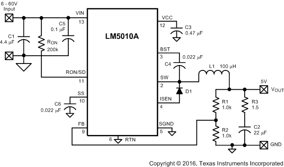 Figure 11. LM5010A Example Circuit
8.2.1 Design Requirements
Table 1 lists the operating parameters for Figure 11.
Table 1. Design Parameters
| PARAMETER | EXAMPLE VALUE |
|---|---|
| Input voltage | 6 V to 60 V |
| Output voltage | 5 V |
| Load current | 200 mA to 1 A |
| Soft-start time | 5 ms |
8.2.2 Detailed Design Procedure
The procedure for calculating the external components is illustrated with a design example. Configure the circuit in Figure 11 according to the components listed in Table 2.
Table 2. List of Components for LM5010A Example Circuit
| ITEM | DESCRIPTION | VALUE |
|---|---|---|
| C1 | Ceramic capacitor | (2) 2.2 µF, 100 V |
| C2 | Ceramic capacitor | 22 µF, 16 V |
| C3 | Ceramic capacitor | 0.47 µF, 16 V |
| C4, C6 | Ceramic capacitor | 0.022 µF, 16 V |
| C5 | Ceramic capacitor | 0.1 µF, 100 V |
| D1 | Schottky diode | 100V, 6 A |
| L1 | Inductor | 100 µH |
| R1 | Resistor | 1 kΩ |
| R2 | Resistor | 1 kΩ |
| R3 | Resistor | 1.5 Ω |
| RON | Resistor | 200 kΩ |
| U1 | LM5010Ax | — |
8.2.2.1 Component Selection
8.2.2.1.1 R1 and R2
These resistors set the output voltage, and calculate their ratio with Equation 10.
R1 and R2 calculates to 1. The resistors should be chosen from standard value resistors in the range of 1 kΩ to 10 kΩ. A value of 1 kΩ is used for R1 and R2.
8.2.2.1.2 RON, FS
RON can be chosen using Equation 7 to set the nominal frequency, or from Equation 6 if the ON-time at a particular VIN is important. A higher frequency generally means a smaller inductor and capacitors (value, size and cost), but higher switching losses. A lower frequency means a higher efficiency, but with larger components. Generally, if PC board space is tight, a higher frequency is better. The resulting ON-time and frequency have a ±25% tolerance. Using Equation 7 at a nominal VIN of 8 V, RON is calculated with Equation 11.

A value of 200 kΩ will be used for RON, yielding a nominal frequency of 161 kHz at VIN = 6 V, and 205 kHz at VIN = 60 V.
8.2.2.1.3 L1
The guideline for choosing the inductor value in this example is that it must keep the circuit’s operation in continuous conduction mode at minimum load current. This is not a strict requirement since the LM5010Ax regulates correctly when in discontinuous conduction mode, although at a lower frequency. However, to provide an initial value for L1 the above guideline will be used. See Figure 12.
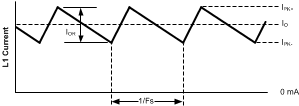 Figure 12. Inductor Current
To keep the circuit in continuous conduction mode, the maximum allowed ripple current is twice the minimum load current, or 400 mAp-p. Using this value of ripple current, the inductor (L1) is calculated using Equation 12 and Equation 13.

where
- FS(min) is the minimum frequency of 154 kHz (205 kHz - 25%) at VIN(max)

Equation 13 provides the minimum value for inductor L1. When selecting an inductor, use a higher standard value (100 uH). To prevent saturation, and possible destructive current levels, L1 must be rated for the peak current which occurs if the current limit and maximum ripple current are reached simultaneously (IPK in Figure 9). The maximum ripple amplitude is calculated by rearranging Equation 12 using VIN(max), FS(min), and the minimum inductor value, based on the manufacturer’s tolerance. Assume for Equation 14, Equation 15, and Equation 16 that the inductor’s tolerance is ±20%.


where
- ILIM is the maximum current limit threshold
At the nominal maximum load current of 1 A, the peak inductor current is 1.186 A.
8.2.2.1.4 RCL
Since it is obvious that the lower peak of the inductor current waveform does not exceed 1 A at maximum load current (see Figure 12), it is not necessary to increase the current limit threshold. Therefore RCL is not needed for this exercise. For applications where the lower peak exceeds 1 A, see Increasing The Current Limit Threshold.
8.2.2.1.5 C1
This capacitor limits the ripple voltage at VIN resulting from the source impedance of the supply feeding this circuit, and the on and off nature of the switch current into VIN. At maximum load current, when the buck switch turns on, the current into VIN steps up from zero to the lower peak of the inductor current waveform (IPK- in Figure 12), ramps up to the peak value (IPK+), then drops to zero at turnoff. The average current into VIN during this ON-time is the load current. For a worst case calculation, C1 must supply this average current during the maximum ON-time. The maximum ON-time is calculated at VIN = 6 V using Equation 5, with a 25% tolerance added in Equation 17.

The voltage at VIN should not be allowed to drop below 5.5 V in order to maintain VCC above its UVLO as in Equation 18.

Normally a lower value can be used for C1 since the above calculation is a worst case calculation which assumes the power source has a high source impedance. A quality ceramic capacitor with a low ESR should be used for C1.
8.2.2.1.6 C2 and R3
Since the LM5010Ax requires a minimum of 25 mVp-p of ripple at the FB pin for proper operation, the required ripple at VOUT is increased by R1 and R2, and is equal to Equation 19.
This necessary ripple voltage is created by the inductor ripple current acting on C2’s ESR + R3. First, the minimum ripple current is determined which occurs at minimum VIN, maximum inductor value, and calculate the maximum frequency with Equation 20.

The minimum ESR for C2 is then equal to Equation 21.

If the capacitor used for C2 does not have sufficient ESR, R3 is added in series as shown in the Block Diagram. The value chosen for C2 is application dependent, and it is recommended that it be no smaller than 3.3 µF. C2 affects the ripple at VOUT, and transient response. Experimentation is usually necessary to determine the optimum value for C2.
8.2.2.1.7 C3
The capacitor at the VCC pin provides noise filtering and stability, prevents false triggering of the VCC UVLO at the buck switch ON and OFF transitions, and limits the peak voltage at VCC when a high voltage with a short rise time is initially applied at VIN. C3 should be no smaller than 0.47 µF, and must be a good quality, low ESR, ceramic capacitor, physically close to the IC pins.
8.2.2.1.8 C4
The recommended value for C4 is 0.022 µF. A high quality ceramic capacitor with low ESR is recommended as C4 supplies the surge current to charge the buck switch gate at each turnon. A low ESR also ensures a complete recharge during each OFF-time.
8.2.2.1.9 C5
This capacitor suppresses transients and ringing due to lead inductance at VIN. TI recommends a low ESR, 0.1 µF ceramic chip capacitor, placed physically close to the LM5010Ax.
8.2.2.1.10 C6
The capacitor at the SS pin determines the soft-start time (that is the time for the reference voltage at the regulation comparator and the output voltage) to reach their final value. Determine the capacitor value with Equation 22.

For a 5 ms soft-start time, C6 calculates to 0.022 µF.
8.2.2.1.11 D1
A Schottky diode is recommended. Ultra-fast recovery diodes are not recommended as the high speed transitions at the SW pin may inadvertently affect the IC’s operation through external or internal EMI. The diode should be rated for the maximum VIN (60 V), the maximum load current (1 A), and the peak current which occurs when current limit and maximum ripple current are reached simultaneously (IPK in Figure 9), previously calculated to be 1.87 A. The diode’s forward voltage drop affects efficiency due to the power dissipated during the OFF-time. The average power dissipation in D1 is calculated from Equation 23.
where
- IO is the load current
- D is the duty cycle
8.2.2.2 Low Output Ripple Configurations
For applications where low output voltage ripple is required the output can be taken directly from the low ESR output capacitor (C2) as shown in Figure 13. However, R3 slightly degrades the load regulation. The specific component values, and the application determine if this is suitable.
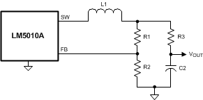 Figure 13. Low Ripple Output
Where the circuit of Figure 13 is not suitable, the circuits of Figure 14 or Figure 15 can be used.
 Figure 14. Low Output Ripple Using a Feed-Forward Capacitor
In Figure 14, Cff is added across R1 to AC-couple the ripple at VOUT directly to the FB pin. This allows the ripple at VOUT to be reduced, in some cases considerably, by reducing R3. In the circuit of Figure 11, the ripple at VOUT ranged from 50 mVp-p at VIN = 6 V to 320 mVp-p at VIN = 60 V. By adding a 1000 pF capacitor at Cff and reducing R3 to 0.75 Ω, the VOUT ripple was reduced by 50%, ranging from 25 mVp-p to 160 mVp-p.
 Figure 15. Low Output Ripple Using Ripple Injection
To reduce VOUT ripple further, the circuit of Figure 15 can be used. R3 has been removed, and the output ripple amplitude is determined by C2’s ESR and the inductor ripple current. RA and CA are chosen to generate a 40 to 50 mVp-p sawtooth at their junction, and that voltage is AC-coupled to the FB pin via CB. In selecting RA and CA, VOUT is considered a virtual ground as the SW pin switches between VIN and –1 V. Since the ON-time at SW varies inversely with VIN, the waveform amplitude at the RA and CA junction is relatively constant. R1 and R2 must typically be increased to more than 10k each to not significantly attenuate the signal provided to FB through CB. Typical values for the additional components are RA = 200 k, CA = 680 pF, and CB = 0.01 µF.
8.2.2.3 Increasing The Current Limit Threshold
The current limit threshold is nominally 1.25 A, with a minimum value of 1 A. If, at maximum load current, the lower peak of the inductor current (IPK- in Figure 12) exceeds 1 A, resistor RCL must be added between SGND and ISEN to increase the current limit threshold to be equal or exceed that lower peak current. This resistor diverts some of the recirculating current from the internal sense resistor so that a higher current level is needed to switch the internal current limit comparator. Calculate IPK- with Equation 24.

where
- IO(max) is the maximum load current
- IOR(min) is the minimum ripple current calculated using Equation 20
RCL is calculated from Equation 25.

where
- 0.11 Ω is the minimum value of the internal resistance from SGND to ISEN
The next smaller standard value resistor must be used for RCL. With the addition of RCL, and when the circuit is in current limit, the upper peak current out of the SW pin (IPK in Figure 9) can be as high as Equation 26.

where
- IOR(max) is calculated using Equation 14
The inductor L1 and diode D1 must be rated for this current. If IPK exceeds 2 A , the inductor value must be increased to reduce the ripple amplitude. This will necessitate recalculation of IOR(min), IPK-, and RCL.
Increasing the circuit’s current limit will increase power dissipation and the junction temperature within the LM5010Ax. See Layout Guidelines for guidelines on this issue.
8.2.3 Application Curves
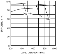 Figure 16. Efficiency vs Load Current and VIN
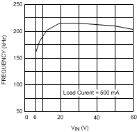 Figure 17. Frequency vs VIN
8.3 Do's and Don'ts
A minimum load current of 500 µA is required to maintain proper operation. If the load current falls below that level, the bootstrap capacitor can discharge during the long OFF-time and the circuit either shuts down or cycles ON and OFF at a low frequency. If the load current is expected to drop below 500 µA in the application, choose the feedback resistors to be low enough in value to provide the minimum required current at nominal VOUT.