SNVS376F October 2005 – May 2016 LM5010A , LM5010A-Q1
PRODUCTION DATA.
- 1 Features
- 2 Applications
- 3 Description
- 4 Revision History
- 5 Pin Configuration and Functions
- 6 Specifications
- 7 Detailed Description
- 8 Application and Implementation
- 9 Power Supply Recommendations
- 10Layout
- 11Device and Documentation Support
- 12Mechanical, Packaging, and Orderable Information
Package Options
Mechanical Data (Package|Pins)
- PWP|14
Thermal pad, mechanical data (Package|Pins)
- PWP|14
Orderable Information
7 Detailed Description
7.1 Overview
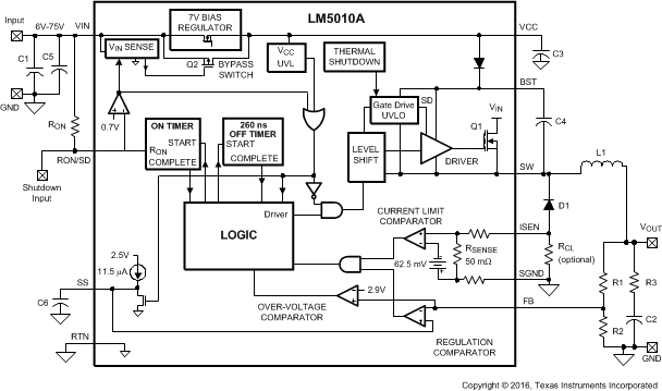
The LM5010Ax step-down switching regulator features all the functions needed to implement a low-cost, efficient, buck bias power converter. This high-voltage regulator contains a 75-V N-channel buck switch, is easy to implement, and is provided in HTSSOP-14 and thermally-enhanced, WSON-10 packages. The regulator is based on a control scheme using an ON-time inversely proportional to VIN. The control scheme requires no loop compensation. The functional block diagram of the LM5010Ax is shown in the Functional Block Diagram.
The LM5010Ax can be applied in numerous applications to efficiently regulate down higher voltages. This regulator is well-suited for 48-V telecom and 42-V automotive power bus ranges. Additional features include: thermal shutdown, VCC undervoltage lockout, gate drive undervoltage lockout, maximum duty cycle limit timer, and the valley current limit functionality.
7.2 Functional Block Diagram

7.3 Feature Description
7.3.1 Control Circuit Overview
The LM5010Ax employs a control scheme based on a comparator and a one-shot ON timer, with the output voltage feedback (FB) compared to an internal reference (2.5 V). If the FB voltage is below the reference the buck switch is turned on for a time period determined by the input voltage and a programming resistor (RON). Following the ON-time the switch remains off for a fixed 260 ns OFF-time, or until the FB voltage falls below the reference, whichever is longer. The buck switch then turns on for another ON-time period. Referring to the Block Diagram, the output voltage is set by R1 and R2. The regulated output voltage is calculated with Equation 1.
The LM5010Ax requires a minimum of 25 mV of ripple voltage at the FB pin for stable fixed-frequency operation. If the output capacitor’s ESR is insufficient, additional series resistance may be required (R3 in the Block Diagram).
The LM5010Ax operates in continuous conduction mode at heavy load currents, and discontinuous conduction mode at light load currents. In continuous conduction mode current always flows through the inductor, never decaying to zero during the OFF-time. In this mode the operating frequency remains relatively constant with load and line variations. The minimum load current for continuous conduction mode is one-half the inductor’s ripple current amplitude. Calculate the operating frequency in the continuous conduction mode with Equation 2.

The buck switch duty cycle is equal to Equation 3.

Under light load conditions, the LM5010Ax operates in discontinuous conduction mode, with zero current flowing through the inductor for a portion of the OFF-time. The operating frequency is always lower than that of the continuous conduction mode, and the switching frequency varies with load current. Conversion efficiency is maintained at a relatively high level at light loads because the switching losses diminish as the power delivered to the load is reduced. Calculate the discontinuous mode operating frequency with Equation 4.

where
- RL is the load resistance
7.3.2 Start-Up Regulator (VCC)
A high voltage bias regulator is integrated within the LM5010Ax. The input pin (VIN) can be connected directly to line voltages between 6 and 75 V. Referring to the block diagram and the graph of VCC vs VIN, when VIN is between 6 V and the bypass threshold (nominally 8.9 V), the bypass switch (Q2) is on, and VCC tracks VIN within 100 mV to 150 mV. The bypass switch on-resistance is approximately 50 Ω, with inherent current limiting at approximately 100 mA. When VIN is above the bypass threshold, Q2 is turned off, and VCC is regulated at 7 V. The VCC regulator output current is limited at approximately 15 mA. When the LM5010Ax is shutdown using the RON/SD pin, the VCC bypass switch is shut off, regardless of the voltage at VIN.
When VIN exceeds the bypass threshold, the time required for Q2 to shut off is approximately 2 to 3 µs. The capacitor at VCC (C3) must be a minimum of 0.47 µF to prevent the voltage at VCC from rising above its absolute maximum rating in response to a step input applied at VIN. C3 must be located as close as possible to the LM5010Ax pins.
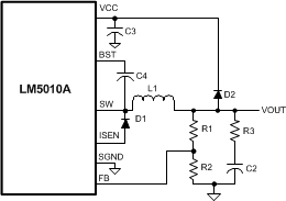
In applications with a relatively high input voltage, power dissipation in the bias regulator is a concern. An auxiliary voltage of between 7.5 V and 14 V can be diode connected to the VCC pin (D2 in Figure 8) to shut off the VCC regulator, reducing internal power dissipation. The current required into the VCC pin is shown in the Typical Performance Characteristics. Internally a diode connects VCC to VIN requiring that the auxiliary voltage be less than VIN.
The turn-on sequence is shown in Figure 1. When VCC exceeds the undervoltage lockout threshold (UVLO) of 5.25 V (t1 in Figure 1), the buck switch is enabled, and the SS pin is released to allow the soft-start capacitor (C6) to charge up. The output voltage VOUT is regulated at a reduced level which increases to the desired value as the soft-start voltage increases (t2 in Figure 1).
 Figure 8. Self Biased Configuration
7.3.3 Regulation Comparator
The feedback voltage at the FB pin is compared to the voltage at the SS pin (2.5 V, ±2%). In normal operation an ON-time period is initiated when the voltage at FB falls below 2.5 V. The buck switch conducts for the ON-time programmed by RON, causing the FB voltage to rise above 2.5 V. After the ON-time period the buck switch remains off until the FB voltage falls below 2.5 V. Input bias current at the FB pin is less than 5 nA over temperature.
7.3.4 Overvoltage Comparator
The feedback voltage at FB is compared to an internal 2.9-V reference. If the voltage at FB rises above 2.9 V the ON-time is immediately terminated. This condition can occur if the input voltage, or the output load, changes suddenly. The buck switch remains off until the voltage at FB falls below 2.5 V.
7.3.5 ON-Time Control
The ON-time of the internal buck switch is determined by the RON resistor and the input voltage (VIN), and is calculated with Equation 5.

The RON resistor can be determined from the desired ON-time by re-arranging Equation 5 to Equation 6.

To set a specific continuous conduction mode switching frequency (fS), the RON resistor is determined with Equation 7.

In high frequency applications the minimum value for tON is limited by the maximum duty cycle required for regulation and the minimum OFF-time of the LM5010Ax (260 ns, ±15%). The fixed OFF-time limits the maximum duty cycle achievable with a low voltage at VIN. The minimum allowed ON-time to regulate the desired VOUT at the minimum VIN is determined with Equation 8.

7.3.6 Soft Start
The soft start feature allows the regulator to gradually reach a steady-state operating point, thereby reducing start-up stresses and current surges. At turnon, while VCC is below the undervoltage threshold (t1 in Figure 1), the SS pin is internally grounded, and VOUT is held at 0 V. When VCC exceeds the undervoltage threshold (UVLO) an internal 11.5-µA current source charges the external capacitor (C6) at the SS pin to 2.5 V (t2 in Figure 1). The increasing SS voltage at the non-inverting input of the regulation comparator gradually increases the output voltage from zero to the desired value. The softstart feature keeps the load inductor current from reaching the current limit threshold during start-up, thereby reducing inrush currents.
An internal switch grounds the SS pin if VCC is below the undervoltage lockout threshold, or if the circuit is shutdown using the RON/SD pin.
7.3.7 N-Channel Buck Switch and Driver
The LM5010Ax integrates an N-Channel buck switch and associated floating high voltage gate driver. The peak current through the buck switch should not exceed 2 A, and the load current should not exceed 1.5 A. The gate driver circuit is powered by the external bootstrap capacitor between BST and SW (C4), which is recharged each OFF-time from VCC through the internal high voltage diode. The minimum OFF-time, nominally 260 ns, ensures sufficient time during each cycle to recharge the bootstrap capacitor. A 0.022-µF ceramic capacitor is recommended for C4.
7.3.8 Current Limit
Current limit detection occurs during the OFF-time by monitoring the recirculating current through the internal current sense resistor (RSENSE). The detection threshold is 1.25 A, ±0.25 A. Referring to Functional Block Diagram, if the current into SGND during the OFF-time exceeds the threshold level the current limit comparator delays the start of the next ON-time period. The next ON-time starts when the current into SGND is below the threshold and the voltage at FB is below 2.5 V. Figure 9 illustrates the inductor current waveform during normal operation and during current limit. The output current IO is the average of the inductor ripple current waveform. The low load current waveform illustrates continuous conduction mode operation with peak and valley inductor currents below the current limit threshold. When the load current is increased (high load current), the ripple waveform maintains the same amplitude and frequency since the current falls below the current limit threshold at the valley of the ripple waveform. Note the average current in the high load current portion of Figure 9 is above the current limit threshold. Since the current reduces below the threshold in the normal OFF-time each cycle, the start of each ON-time is not delayed, and the circuit’s output voltage is regulated at the correct value. When the load current is further increased such that the lower peak would be above the threshold, the OFF-time is lengthened to allow the current to decrease to the threshold before the next ON-time begins (Current Limited portion of Figure 9). Both VOUT and the switching frequency are reduced as the circuit operates in a constant current mode. The load current (IOCL) is equal to the current limit threshold plus half the ripple current (ΔI/2). The ripple amplitude (ΔI) is calculated with Equation 9.

The current limit threshold can be increased by connecting an external resistor (RCL) between SGND and ISEN. RCL typically is less than 1 Ω, and the calculation of its value is explained in Application and Implementation. If the current limit threshold is increased by adding RCL, the maximum continuous load current should not exceed 1.5 A, and the peak current out of the SW pin should not exceed 2 A.
 Figure 9. Inductor Current, Current Limit Operation
7.3.9 Thermal Shutdown
The LM5010Ax should be operated below the maximum operating junction temperature rating. If the junction temperature increases during a fault or abnormal operating condition, the internal thermal shutdown circuit activates typically at 175°C. The Thermal Shutdown circuit reduces power dissipation by disabling the buck switch and the ON timer. This feature helps prevent catastrophic failures from accidental device overheating. When the junction temperature reduces below approximately 155°C (20°C typical hysteresis), normal operation resumes.
7.4 Device Functional Modes
7.4.1 Shutdown
The LM5010Ax can be remotely shut down by forcing the RON/SD pin below 0.7 V with a switch or open drain device. See Figure 10. In the shutdown mode the SS pin is internally grounded, the ON-time one-shot is disabled, the input current at VIN is reduced, and the VCC bypass switch is turned off. The VCC regulator is not disabled in the shutdown mode. Releasing the RON/SD pin allows normal operation to resume. The nominal voltage at RON/SD is shown in the Typical Performance Characteristics. When switching the RON/SD pin, the transition time should be faster than one to two cycles of the regulator’s nominal switching frequency.
 Figure 10. Shutdown Implementation