SNVSCB3 October 2022 LM5013
PRODUCTION DATA
- 1 Features
- 2 Applications
- 3 Description
- 4 Revision History
- 5 Device Comparison Table
- 6 Pin Configuration and Functions
- 7 Specifications
-
8 Detailed Description
- 8.1 Overview
- 8.2 Functional Block Diagram
- 8.3
Feature Description
- 8.3.1 Control Architecture
- 8.3.2 Internal VCC Regulator and Bootstrap Capacitor
- 8.3.3 Regulation Comparator
- 8.3.4 Internal Soft Start
- 8.3.5 On-Time Generator
- 8.3.6 Current Limit
- 8.3.7 N-Channel Buck Switch and Driver
- 8.3.8 Schottky Diode Selection
- 8.3.9 Enable and Undervoltage Lockout (EN/UVLO)
- 8.3.10 Power Good (PGOOD)
- 8.3.11 Thermal Protection
- 8.4 Device Functional Modes
- 9 Application and Implementation
- 10Device and Documentation Support
- 11Mechanical, Packaging, and Orderable Information
Package Options
Mechanical Data (Package|Pins)
- DDA|8
Thermal pad, mechanical data (Package|Pins)
- DDA|8
Orderable Information
9.3 Power Supply Recommendations
The LM5013 buck converter is designed to operate from a wide input voltage range between 6 V and 100 V. In addition, the input supply must be capable of delivering the required input current to the fully-loaded regulator. Use Equation 19 to estimate the average input current.
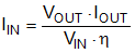
where
- η is the efficiency.
If the converter is connected to an input supply through long wires or PCB traces with a large impedance, take special care to achieve stable performance. The parasitic inductance and resistance of the input cables can have an adverse effect on converter operation. The parasitic inductance in combination with the low-ESR ceramic input capacitors form an underdamped resonant circuit. This circuit can cause overvoltage transients at VIN each time the input supply is cycled ON and OFF. The parasitic resistance causes the input voltage to dip during a load transient. If the converter is operating close to the minimum input voltage, this dip can cause false UVLO fault triggering and a system reset, in addition to potential stability issues. The circuit can be damped with a "parallel damping network." For example, a 22-μF damping capacitor in series with a 1.4-Ω resistor connected to the VIN node, creates a parallel damped network, providing sufficient damping for a 8.2-μH input filter inductor and 4.4-μF ceramic input capacitance. Damping is not only needed for an input EMC filter, but also when the application utilizes a power harness, which can present a large input loop inductance. For example, two cables (one for VIN and one for GND), each one meter (approximately three feet) long with approximately 1-mm diameter (18 AWG), placed 1 cm (approximately 0.4 inch) apart forms a rectangular loop resulting in about 1.2 µH of inductance. The Input Filter Design for Switching Power Supplies application report provides more detail on this topic.
An EMI input filter is often used in front of the regulator that, unless carefully designed, can lead to instability as well as some of the effects mentioned above. The Simple Success with Conducted EMI for DC-DC Converters application report provides helpful suggestions when designing an input filter for any switching regulator.