SNVS788H January 2012 – August 2021 LM5019
PRODUCTION DATA
- 1 Features
- 2 Applications
- 3 Description
- 4 Revision History
- 5 Pin Configuration and Functions
- 6 Specifications
-
7 Detailed Description
- 7.1 Overview
- 7.2 Functional Block Diagram
- 7.3
Feature Description
- 7.3.1 Control Overview
- 7.3.2 VCC Regulator
- 7.3.3 Regulation Comparator
- 7.3.4 Overvoltage Comparator
- 7.3.5 On-Time Generator
- 7.3.6 Current Limit
- 7.3.7 N-Channel Buck Switch and Driver
- 7.3.8 Synchronous Rectifier
- 7.3.9 Undervoltage Detector
- 7.3.10 Thermal Protection
- 7.3.11 Ripple Configuration
- 7.3.12 Soft Start
- 7.4 Device Functional Modes
-
8 Application and Implementation
- 8.1 Application Information
- 8.2
Typical Applications
- 8.2.1 Application Circuit: 12.5 V to 95 V Input and 10 V, 100-mA Output Buck Converter
- 8.2.2
Application Circuit: 20 V to 95 V Input and 10 V, 100 mA Output Isolated
Fly-Buck Converter
- 8.2.2.1 Design Requirements
- 8.2.2.2
Detailed Design Procedure
- 8.2.2.2.1 Transformer Turns Ratio
- 8.2.2.2.2 Total IOUT
- 8.2.2.2.3 RFB1, RFB2
- 8.2.2.2.4 Frequency Selection
- 8.2.2.2.5 Transformer Selection
- 8.2.2.2.6 Primary Output Capacitor
- 8.2.2.2.7 Secondary Output Capacitor
- 8.2.2.2.8 Type III Feedback Ripple Circuit
- 8.2.2.2.9 Secondary Diode
- 8.2.2.2.10 VCC and Bootstrap Capacitor
- 8.2.2.2.11 Input Capacitor
- 8.2.2.2.12 UVLO Resistors
- 8.2.2.2.13 VCC Diode
- 8.2.2.3 Application Curves
- 9 Power Supply Recommendations
- 10Layout
- 11Device and Documentation Support
- 12Mechanical, Packaging, and Orderable Information
Package Options
Mechanical Data (Package|Pins)
Thermal pad, mechanical data (Package|Pins)
- DDA|8
Orderable Information
8.2.1.2.6 Type II Ripple Circuit
Type II ripple circuit as described in Section 7.3.11 is chosen for this example. For a constant on-time converter to be stable, the injected in-phase ripple must be larger than the capacitive ripple on COUT.
Using type II ripple circuit equations with minimum FB pin ripple of 25 mV, the values of the series resistor RC and ac coupling capacitor Cac can calculated.
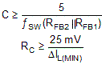
Assuming RFB2 = 6.98 kΩ and RFB1 = 1 kΩ, the calculated minimum value of Cac is 0.013 µF. A standard value of 0.1 µF is selected for Cac = C8. The value of the series output resistor RC is calculated for the minimum input voltage condition when the inductor ripple current as at a minimum. Using Equation 11 and assuming VIN = 12.5 V, the minimum inductor ripple current is 27 mA. The calculated minimum value of RC is 0.93 Ω. A standard value of 1.5 Ω is selected for RC = R2 to provide additional ripple for stable switching at low VIN.