SNVSAG9 March 2016 LM5022-Q1
PRODUCTION DATA.
- 1 Features
- 2 Applications
- 3 Description
- 4 Revision History
- 5 Pin Configuration and Functions
- 6 Specifications
- 7 Detailed Description
-
8 Application and Implementation
- 8.1 Application Information
- 8.2
Typical Application
- 8.2.1 Design Requirements
- 8.2.2
Detailed Design Procedure
- 8.2.2.1 Switching Frequency
- 8.2.2.2 MOSFET
- 8.2.2.3 Output Diode
- 8.2.2.4 Boost Inductor
- 8.2.2.5 Output Capacitor
- 8.2.2.6 VCC Decoupling Capacitor
- 8.2.2.7 Input Capacitor
- 8.2.2.8 Current Sense Filter
- 8.2.2.9 RSNS, RS2 and Current Limit
- 8.2.2.10 Control Loop Compensation
- 8.2.2.11 Efficiency Calculations
- 8.2.3 Application Curves
- 9 Power Supply Recommendations
- 10Layout
- 11Device and Documentation Support
- 12Mechanical, Packaging, and Orderable Information
Package Options
Mechanical Data (Package|Pins)
- DGS|10
Thermal pad, mechanical data (Package|Pins)
Orderable Information
7 Detailed Description
7.1 Overview
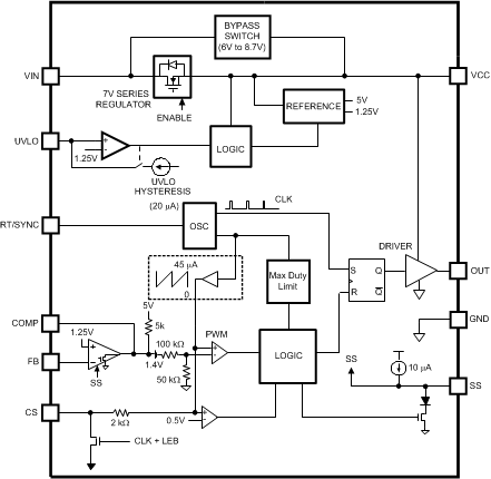
The LM5022-Q1 is a low-side N-channel MOSFET controller that contains all of the features needed to implement single ended power converter topologies. The LM5022-Q1 includes a high-voltage startup regulator that operates over a wide input range of 6 V to 60 V. The PWM controller is designed for high speed capability including an oscillator frequency range up to 2.2 MHz and total propagation delays less than 100 ns. Additional features include an error amplifier, precision reference, input under-voltage lockout, cycle-by-cycle current limit, slope compensation, soft-start, oscillator sync capability and thermal shutdown.
The LM5022-Q1 is designed for current-mode control power converters that require a single drive output, such as boost and SEPIC topologies. The LM5022-Q1 provides all of the advantages of current-mode control including input voltage feed-forward, cycle-by-cycle current limiting and simplified loop compensation.
7.2 Functional Block Diagram

7.3 Feature Description
7.3.1 High Voltage Start-Up Regulator
The LM5022-Q1 contains an internal high-voltage start-up regulator that allows the VIN pin to be connected directly to line voltages as high as 60 V. The regulator output is internally current limited to 35 mA (typical). When power is applied, the regulator is enabled and sources current into an external capacitor, CF, connected to the VCC pin. The recommended capacitance range for CF is 0.1 µF to 100 µF. When the voltage on the VCC pin reaches the rising threshold of 5 V, the controller output is enabled. The controller will remain enabled until VCC falls below 4.7 V. In applications using a transformer, an auxiliary winding can be connected through a diode to the VCC pin. This winding should raise the VCC pin voltage to above 7.5 V to shut off the internal startup regulator. Powering VCC from an auxiliary winding improves conversion efficiency while reducing the power dissipated in the controller. The capacitance of CF must be high enough that it maintains the VCC voltage greater than the VCC UVLO falling threshold (4.7 V) during the initial start-up. During a fault condition when the converter auxiliary winding is inactive, external current draw on the VCC line should be limited such that the power dissipated in the start-up regulator does not exceed the maximum power dissipation capability of the controller.
An external start-up or other bias rail can be used instead of the internal start-up regulator by connecting the VCC and the VIN pins together and feeding the external bias voltage (7.5 V to 14 V) to the two pins.
7.3.2 Input Undervoltage Detector
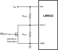
The LM5022-Q1 contains an input undervoltage lockout (UVLO) circuit. UVLO is programmed by connecting the UVLO pin to the center point of an external voltage divider from VIN to GND. The resistor divider must be designed such that the voltage at the UVLO pin is greater than 1.25 V when VIN is in the desired operating range. If the under voltage threshold is not met, all functions of the controller are disabled and the controller remains in a low power standby state. UVLO hysteresis is accomplished with an internal 20 µA current source that is switched on or off into the impedance of the set-point divider. When the UVLO threshold is exceeded, the current source is activated to instantly raise the voltage at the UVLO pin. When the UVLO pin voltage falls below the 1.25 V threshold the current source is turned off, causing the voltage at the UVLO pin to fall. The UVLO pin can also be used to implement a remote enable / disable function. If an external transistor pulls the UVLO pin below the 1.25 V threshold, the converter will be disabled. This external shutdown method is shown in Figure 12.
 Figure 12. Enable/Disable Using UVLO
7.3.3 Error Amplifier
An internal high gain error amplifier is provided within the LM5022-Q1. The amplifier’s non-inverting input is internally set to a fixed reference voltage of 1.25 V. The inverting input is connected to the FB pin. In non-isolated applications such as the boost converter the output voltage, VO, is connected to the FB pin through a resistor divider. The control loop compensation components are connected between the COMP and FB pins. For most isolated applications the error amplifier function is implemented on the secondary side of the converter and the internal error amplifier is not used. The internal error amplifier is configured as an open drain output and can be disabled by connecting the FB pin to ground. An internal 5-kΩ pullup resistor between a 5-V reference and COMP can be used as the pull-up for an opto-coupler in isolated applications.
7.3.4 Current Sensing and Current Limiting
The LM5022-Q1 provides a cycle-by-cycle over current protection function. Current limit is accomplished by an internal current sense comparator. If the voltage at the current sense comparator input exceeds 0.5 V, the MOSFET gate drive will be immediately terminated. A small RC filter, located near the controller, is recommended to filter noise from the current sense signal. The CS input has an internal MOSFET which discharges the CS pin capacitance at the conclusion of every cycle. The discharge device remains on an additional 65 ns after the beginning of the new cycle to attenuate leading edge ringing on the current sense signal.
The LM5022-Q1 current sense and PWM comparators are very fast, and may respond to short duration noise pulses. Layout considerations are critical for the current sense filter and sense resistor. The capacitor associated with the CS filter must be located very close to the device and connected directly to the pins of the controller (CS and GND). If a current sense transformer is used, both leads of the transformer secondary should be routed to the sense resistor and the current sense filter network. The current sense resistor can be located between the source of the primary power MOSFET and power ground, but it must be a low inductance type. When designing with a current sense resistor all of the noise sensitive low-power ground connections should be connected together locally to the controller and a single connection should be made to the high current power ground (sense resistor ground point).
7.3.5 PWM Comparator and Slope Compensation
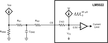
The PWM comparator compares the current ramp signal with the error voltage derived from the error amplifier output. The error amplifier output voltage at the COMP pin is offset by 1.4 V and then further attenuated by a 3:1 resistor divider. The PWM comparator polarity is such that 0 V on the COMP pin will result in a zero duty cycle at the controller output. For duty cycles greater than 50%, current mode control circuits can experience sub-harmonic oscillation. By adding an additional fixed-slope voltage ramp signal (slope compensation) this oscillation can be avoided. Proper slope compensation damps the double pole associated with current mode control (see Control Loop Compensation) and eases the design of the control loop compensator. The LM5022-Q1 generates the slope compensation with a sawtooth-waveform current source with a slope of 45 µA × ƒSW, generated by the clock (see Figure 13). This current flows through an internal 2-kΩ resistor to create a minimum compensation ramp with a slope of 100 mV × ƒSW (typical). The slope of the compensation ramp increases when external resistance is added for filtering the current sense (RS1) or in the position RS2. As shown in Figure 13 and the Functional Block Diagram, the sensed current slope and the compensation slope add together to create the signal used for current limiting and for the control loop itself.
 Figure 13. Slope Compensation
In peak current mode control the optimal slope compensation is proportional to the slope of the inductor current during the power switch off-time. For boost converters the inductor current slope while the MOSFET is off is (VO - VIN) / L. This relationship is combined with the requirements to set the peak current limit and is used to select RSNS and RS2 in Application and Implementation.
7.3.6 Soft Start
The soft-start feature allows the power converter output to gradually reach the initial steady state output voltage, thereby reducing start-up stresses and current surges. At power on, after the VCC and input under-voltage lockout thresholds are satisfied, an internal 10-µA current source charges an external capacitor connected to the SS pin. The capacitor voltage will ramp up slowly and will limit the COMP pin voltage and the switch current.
7.3.7 MOSFET Gate Driver
The LM5022-Q1 provides an internal gate driver through the OUT pin that can source and sink a peak current of 1 A to control external, ground-referenced N-channel MOSFETs.
7.3.8 Thermal Shutdown
Internal thermal shutdown circuitry is provided to protect the LM5022-Q1 in the event that the maximum junction temperature is exceeded. When activated, typically at 165°C, the controller is forced into a low power standby state, disabling the output driver and the VCC regulator. After the temperature is reduced (typical hysteresis is 25°C) the VCC regulator will be re-enabled and the LM5022-Q1 will perform a soft start.
7.4 Device Functional Modes
7.4.1 Oscillator, Shutdown, and SYNC
A single external resistor, RT, connected between the RT/SYNC and GND pins sets the LM5022-Q1 oscillator frequency. To set the switching frequency, ƒSW, RT can be calculated from:
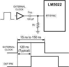
The LM5022-Q1 can also be synchronized to an external clock. The external clock must have a higher frequency than the free running oscillator frequency set by the RT resistor. The clock signal should be capacitively coupled into the RT/SYNC pin with a 100-pF capacitor as shown in Figure 14. A peak voltage level greater than 3.8 V at the RT/SYNC pin is required for detection of the sync pulse. The sync pulse width should be set between 15 ns to 150 ns by the external components. The RT resistor is always required, whether the oscillator is free running or externally synchronized. The voltage at the RT/SYNC pin is internally regulated to 2 V, and the typical delay from a logic high at the RT/SYNC pin to the rise of the OUT pin voltage is 120 ns. RT should be located very close to the device and connected directly to the pins of the controller (RT/SYNC and GND).
 Figure 14. SYNC Operation
