SNVS363E August 2005 – November 2015 LM5026
PRODUCTION DATA.
- 1 Features
- 2 Applications
- 3 Description
- 4 Revision History
- 5 Pin Configuration and Functions
- 6 Specifications
-
7 Detailed Description
- 7.1 Overview
- 7.2 Functional Block Diagram
- 7.3
Feature Description
- 7.3.1 High Voltage Start-Up Regulator
- 7.3.2 Line Undervoltage Detector
- 7.3.3 PWM Outputs
- 7.3.4 Gate Driver Outputs
- 7.3.5 PWM Comparator/Slope Compensation
- 7.3.6 Maximum Duty Cycle Clamp
- 7.3.7 Soft-Start / Soft-Stop
- 7.3.8 Current Sense and Current Limit
- 7.3.9 Overload Protection Timer
- 7.3.10 Oscillator and Sync Capability
- 7.3.11 Thermal Protection
- 7.4 Device Functional Modes
-
8 Application and Implementation
- 8.1 Application Information
- 8.2 Typical Application
- 9 Power Supply Recommendations
- 10Layout
- 11Device and Documentation Support
- 12Mechanical, Packaging, and Orderable Information
Package Options
Mechanical Data (Package|Pins)
Thermal pad, mechanical data (Package|Pins)
Orderable Information
7 Detailed Description
7.1 Overview
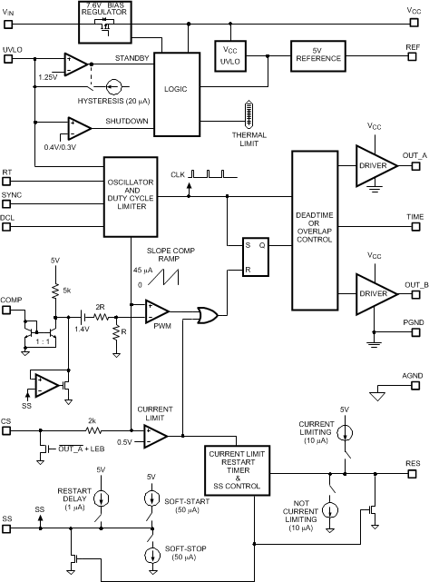
The LM5026 PWM controller contains all of the features necessary to implement power converters utilizing the active clamp reset technique with current mode control. With the active clamp reset, higher efficiencies and greater power densities can be realized compared to conventional catch winding or RDC clamp reset techniques. The LM5026 provides two control outputs, the main power switch control (OUT_A) and the active clamp switch control (OUT_B). The device can be configured to drive either a P-Channel or N-Channel clamp switch. The main switch gate driver features a compound configuration consisting of both MOS and bipolar devices, which provide superior gate drive characteristics. The LM5026 can be configured to operate with bias voltages over a wide input range from 8 V to 100 V. Additional features include programmable maximum duty cycle, line undervoltage lockout, cycle-by-cycle current limit, hiccup mode fault protection with adjustable delays, PWM slope compensation, soft-start, a 1-MHz capable oscillator with synchronization input and output capability, precision reference, and thermal shutdown.
7.2 Functional Block Diagram
7.3 Feature Description
7.3.1 High Voltage Start-Up Regulator
The LM5026 contains an internal high voltage start-up regulator that allows the input pin (VIN) to be connected directly to a nominal 48-V DC line voltage. The regulator output (VCC) is internally current limited to 20 mA. When power is applied and the UVLO pin potential is greater than 0.4 V, the regulator is enabled and sources current into an external capacitor connected to the VCC pin. The recommended capacitance range for the VCC regulator is 0.1 µF to 100 µF. The VCC regulator provides power to the internal voltage reference, PWM controller and gate drivers. The controller outputs are enabled when the voltage on the VCC pin reaches the regulation point of 7.6 V, the internal voltage reference (REF) reaches its regulation point of 5 V and the UVLO voltage is greater than 1.25 V. In typical applications, an auxiliary transformer winding is connected through a diode to the VCC pin. This winding must raise the VCC voltage above 8 V to shut off the internal start-up regulator. Powering VCC from an auxiliary winding improves efficiency while reducing the controller’s power dissipation.
The external VCC capacitor must be sized such that the current delivered from the capacitor and the VCC regulator will maintain a VCC voltage greater than 6.2 V during the initial start-up. During a fault mode when the converter auxiliary winding is inactive, external current draw on the VCC line should be limited such that the power dissipated in the start-up regulator does not exceed the maximum power dissipation of the IC package. An external start-up or bias regulator can be used to power the LM5026 instead of the internal start-up regulator by connecting the VCC and the VIN pins together and connecting an external bias supply to these two pins.
7.3.2 Line Undervoltage Detector
The LM5026 contains a dual level undervoltage lockout (UVLO) circuit. When the UVLO pin voltage is below 0.4 V, the controller is in a low current shutdown mode. When the UVLO pin voltage is greater than 0.4 V but less than 1.25 V, the controller is in standby mode. In standby mode the VCC and REF bias regulators are active while the controller outputs are disabled. When the VCC and REF outputs exceed the VCC and REF undervoltage thresholds and the UVLO pin voltage is greater than 1.25 V, the outputs are enabled and normal operation begins. An external set-point voltage divider from VIN to GND can be used to set the operational range of the converter. The divider must be designed such that the voltage at the UVLO pin will be greater than 1.25 V when VIN is in the desired operating range. UVLO hysteresis is accomplished with an internal 20-µA current source that is switched on or off into the impedance of the set-point divider. When the UVLO threshold is exceeded, the current source is activated to instantly raise the voltage at the UVLO pin. When the UVLO pin voltage falls below the 1.25-V threshold, the current source is turned off causing the voltage at the UVLO pin to fall. The hysteresis of the 0.4-V shutdown comparator is fixed at 100 mV.
The UVLO pin can also be used to implement various remote enable and disable functions. Pulling the UVLO pin below the 0.4-V threshold totally disables the controller. Pulling the UVLO pin to a potential between 1.25 and 0.4 V places the controller in standby with the VCC and REF regulators operating. Turning off a converter by forcing the UVLO pin to the standby condition provides a controlled soft-stop. The controller outputs are not directly disabled in standby mode, rather the soft-start capacitor is discharged with a 50-µA sink current. Discharging the soft-start capacitor gradually reduces the PWM duty cycle to zero, providing a slow controlled discharge of the power converter output filter. This controlled discharge can help prevent uncontrolled behavior of self-driven synchronous rectifiers during turnoff.
7.3.3 PWM Outputs
The relative phase of the main switch gate driver OUT_A and active clamp gate driver OUT_B can be configured for multiple applications. For active clamp configurations utilizing a ground referenced P-Channel clamp switch, the two outputs should be in phase, with the active clamp output overlapping the main output. For active clamp configurations utilizing a high-side N-Channel switch, the active clamp output should be out of phase with main output and there should be a dead time between the two gate drive pulses. A distinguishing feature of the LM5026 is the ability to accurately configure either deadtime (both off) or overlap time (both on) of the gate driver outputs. The overlap / deadtime magnitude is controlled by the resistor value (RSET) connected to the TIME pin of the controller. The opposite end of the resistor can be connected to either REF for deadtime control or to AGND for overlap control. The internal configuration detector senses the direction of current flow in the TIME pin resistor and configures the phase relationship of the main and active clamp outputs.
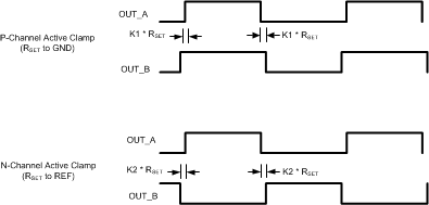 Figure 14. PWM Output Phasing / Timing
The rising edge overlap or deadtime and the falling edge overlap or deadtime are identical and are independent of operating frequency or duty cycle. The magnitude of the overlap/deadtime can be calculated in Equation 1 and Equation 2:
where
- RSET in kΩ
- overlap is in ns
.
where
- RSET in kΩ
- deadtime is in ns
7.3.4 Gate Driver Outputs
The LM5026 provides two-gate driver outputs, the main power switch control (OUT_A) and the active clamp switch control (OUT_B). The main gate driver features a compound configuration, consisting of both MOS and bipolar devices, which provide superior gate drive characteristics. The bipolar device provides most of the drive current capability and sinks a relatively constant current, which is ideal for driving large-power MOSFETs. As the switching event nears conclusion and the bipolar device saturates, the internal MOS device provides a low impedance to compete the switching event.
During turnoff at the Miller plateau region, typically between 2 V to 4 V, the voltage differential between the output and PGND is small and the current source characteristic of the bipolar device is beneficial to reduce the transition time. During turnon, the resistive characteristics of a purely MOS gate driver is adequate since the supply to output voltage differential is fairly large in the Miller region.
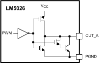 Figure 15. Compound Gate Driver
7.3.5 PWM Comparator/Slope Compensation
The PWM comparator modulates the pulse width of the controller output by comparing the current sense ramp signal to the loop error signal. This comparator is optimized for speed in order to achieve minimum controllable duty cycles. The loop error signal is input into the controller in the form of a control current into the COMP pin. The COMP pin control current is internally mirrored by a matched pair of NPN transistors which sink current through a 5-kΩ resistor connected to the 5-V reference. The resulting error signal passes through a 1.4-V level shift and a gain reducing 3:1 resistor divider before being applied to the pulse width modulator.
The optocoupler detector can be connected between the REF pin and the COMP pin. Because the COMP pin is controlled by a current input, the potential difference across the optocoupler detector is nearly constant. The bandwidth limiting phase delay which is normally introduced by the significant capacitance of the optocoupler is greatly reduced. Greater system loop bandwidth can be realized, since the bandwidth-limiting pole associated with the optocoupler is now at a much higher frequency. The PWM comparator polarity is configured such that with no current into the COMP pin, the controller produces the maximum duty cycle at the main gate driver output.
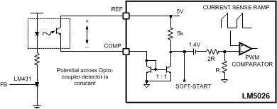 Figure 16. Optocoupler to LM5026 COMP Interface
For duty cycles greater than 50 percent, current mode control circuits are subject to sub-harmonic oscillation. By adding an additional fixed slope voltage ramp signal (slope compensation) to the current sense signal, this oscillation can be avoided. The LM5026 integrates this slope compensation by summing a current ramp generated by the oscillator with the current sense signal. The PWM comparator ramp signal is a combination of the current waveform at the CS pin, and an internally generated slope compensation ramp derived from the oscillator. The internal ramp has an amplitude of 0 to 45 µA which is sourced into an internal 2-kΩ resistor, plus the external impedance at the CS pin. Additional slope compensation may be added by increasing the source impedance of the current sense signal.
7.3.6 Maximum Duty Cycle Clamp
Controlling the maximum duty cycle of an active clamp reset PWM controller is necessary to limit the voltage stress on the main and active clamp MOSFETs. The relationship between the maximum drain-source voltage of the MOSFETs and the maximum PWM duty cycle is provided by Equation 3:

The main output (OUT_A) duty cycle is normally controlled by the control current sourced into the COMP pin from the external feedback circuit. When the feedback demands maximum output from the converter, the duty cycle will be limited by one of two circuits within the LM5026: the user programmable duty cycle clamp and the voltage-dependent duty cycle limiter, which varies inversely with the input line voltage.
Programmable Duty Cycle Clamp – The maximum allowed duty cycle can be programmed by setting a voltage at the DCL pin to a value less than 2 V. The recommended method to set the DCL pin voltage is with a resistor divider connected from the RT pin to AGND. The voltage at the RT pin is internally regulated to 2 V, while the current sourced from the RT pin sets the oscillator frequency. The maximum duty can be programmed, according to Equation 4:

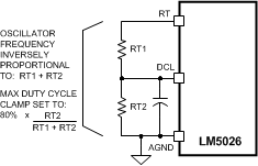 Figure 17. Programming Oscillator Frequency and Maximum Duty Cycle Clamp
Line Voltage Duty Cycle Limiter - The maximum duty cycle for the main output driver is also limited by the voltage at the UVLO pin, which is normally proportional to VIN. The controller outputs are disabled until the UVLO pin voltage exceeds 1.25 V. At the minimum operating voltage (when UVLO = 1.25 V) the maximum duty cycle starts at the duty cycle clamp level programmed by the DCL pin voltage (80% or less). As the line voltage increases, the maximum duty cycle decreases linearly with increasing UVLO voltage, as shown in Figure 18. Ultimately the duty cycle of the main output is controlled to the least of the following three variables: the duty cycle controlled by the PWM comparator, the programmable maximum duty cycle clamp, or the line voltage dependent duty cycle limiter.
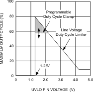 Figure 18. Maximum Duty Cycle vs UVLO Voltage
7.3.7 Soft-Start / Soft-Stop
The soft-start circuit allows the regulator to gradually reach a steady-state operating point, thereby reducing start-up stresses and current surges. Upon turnon, the SS pin capacitor is discharged by an internal switch. When the UVLO, VCC and REF pins reach their operating thresholds, the SS capacitor is released and charged with a 50-µA current source. The PWM comparator control voltage is clamped to the SS pin voltage. When the PWM input reaches 1.4 V, output pulses commence with slowly increasing duty cycle. The voltage at the SS pin eventually increases to 5 V, while the voltage at the PWM comparator increases to the value required for regulation determined by the voltage feedback loop.
If the UVLO pin voltage falls below the 1.25-V standby threshold but above the 0.4-V shutdown threshold, the 50-µA SS pin source current is disabled and a 50-µA sink current discharges the soft-start capacitor. As the SS voltage falls and clamps the PWM comparator input, the PWM duty cycle will gradually fall to zero. This soft-stop feature produces a gradual reduction of the power converter output voltage. This gradual discharge of the output filter prevents oscillations in the self-driven synchronous rectifiers on the secondary side of the converter during turnoff.
7.3.8 Current Sense and Current Limit
The CS input provides a control ramp for the pulse width modulator and current limit detection for overload protection. If the sensed voltage at the CS comparator exceeds 0.5 V, the present cycle is terminated (cycle-by-cycle current limit mode).
A small RC filter, located near the controller, is recommended for the CS input pin. An internal FET connected to the CS input discharges the current sense filter capacitor at the conclusion of every cycle to improve dynamic performance. This same FET remains on for an additional 100 nS at the start of each main switch cycle to attenuate the leading edge spike in the current sense signal.
The CS comparator is very fast and may respond to short duration noise pulses. Layout considerations are critical for the current sense filter and sense resistor. The capacitor associated with the CS filter must be placed very close to the device and connected directly to the pins of the LM5026 (CS and AGND pins). If a current sense transformer is used, both leads of the transformer secondary should be routed to the filter network, which should be located close to the IC. If a sense resistor located in the source of the main switch MOSFET is used for current sensing, a low inductance type of resistor is required. When designing with a current sense resistor, all of the noise-sensitive, low-power ground connections should be connected together near the AGND pin and a single connection should be made to the power ground (sense resistor ground point).
7.3.9 Overload Protection Timer
The LM5026 provides a current limit restart timer to disable the outputs and force a delayed restart (hiccup mode) if a current limit condition is repeatedly sensed. The number of cycle-by-cycle current limit events required to trigger the restart is programmable by means of an external capacitor at the RES pin. During each PWM cycle the LM5026 either sources or sinks current from the RES pin capacitor. If no current limit is detected during a cycle, a 10-µA discharge current sink is enabled to hold the RES pin at ground. If a current limit is detected, the 10-µA sink current is disabled and a 10-µA current source causes the voltage at RES pin to gradually increase. In the event of an extended overload condition, the LM5026 protects the converter with cycle-by-cycle current limiting while the voltage at RES pin increases. If the RES voltage reaches the 2.5-V threshold, the following restart sequence occurs (see Figure 19):
- The RES capacitor and SS capacitors are fully discharged.
- The soft-start current source is reduced from 50 µA to 1 µA
- The SS capacitor voltage slowly increases. When the SS voltage reaches 1.4 V, the PWM comparator will produce the first output pulse. After the first pulse occurs, the SS source current reverts to the normal 50 µA level. The SS voltage increases at its normal rate gradually increasing the duty cycle of the output drivers
- If the overload condition persists after restart, cycle-by-cycle current limiting will cause the voltage on the RES capacitor to increase again, repeating the hiccup mode sequence.
- If the overload condition no longer exists after restart, the RES pin will be held at ground by the 10-µA current sink and normal operation resumes.
The overload timer function is very versatile and can be configured for the following modes of protection:
- Cycle-by-cycle only: The hiccup mode can be completely disabled by connecting the RES pin to AGND. In this configuration, the cycle-by-cycle protection will limit the output current indefinitely and no hiccup sequences will occur.
- Hiccup only: The timer can be configured for immediate activation of a hiccup sequence upon detection of an overload by leaving the RES pin open circuit.
- Delayed Hiccup: The most common configuration as previously described, is a programmed interval of cycle-by-cycle limiting before initiating a hiccup mode restart. The advantage of this configuration is short-term overload conditions will not cause a hiccup mode restart, however during extended overload conditions the average dissipation of the power converter will be very low.
- Externally Controlled Hiccup: The RES pin can also be used as an input. By externally driving the pin to a level greater than the 2.5-V hiccup threshold, the controller will be forced into the delayed restart sequence. If the RES pin is used as an input, the driving source should be current limited to less than 5 mA. For example, the external trigger for a delayed restart sequence could come an overtemperature protection circuit.
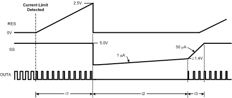 Figure 19. Hiccup Overload Restart Timing
7.3.10 Oscillator and Sync Capability
The LM5026 oscillator frequency is set by the external resistance connected between the RT pin and ground (AGND). To set a desired oscillator frequency (F) the necessary value of total RT resistance can be calculated from Equation 5:

The RT resistor(s) should be located very close to the device and connected directly to the pins of the IC (RT and AGND).
The SYNC pin can be used to synchronize the internal oscillator to an external clock. An open drain output is the recommended interface between the external clock to the LM5026 SYNC pin as illustrated in Figure 20. The clock pulse width must be greater than 15 ns. The external clock frequency must be a higher than the free running frequency set by the RT resistance.
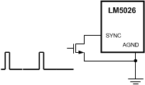 Figure 20. Sync from External Clock
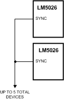 Figure 21. Sync from Multiple Devices
Multiple LM5026 devices can be synchronized together simply by connecting the devices SYNC pins together as shown in Figure 21. Take care to ensure the ground potential differences between devices are minimized. In this configuration all of the devices will be synchronized to the highest frequency device. The internal block diagram of the oscillator and synchronization circuit is shown in Figure 22. The SYNC I/O pin is a CMOS buffer with pullup current limited to 200 µA. If an external device forces the SYNC pin low before the internal oscillator ramp completes its charging cycle, the ramp will be reset and another cycle begins. If the SYNC pins of multiple LM5026 devices are connected together, the first SYNC pin that pulls low will reset the oscillator RAMP of all other devices. All controllers will operate in phase when synchronized using the SYNC I/O feature. Up to five LM5026 devices can be synchronized using this technique.
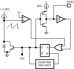 Figure 22. Oscillator Sync I/O Block Diagram
7.3.11 Thermal Protection
Internal Thermal Shutdown circuitry is provided to protect the integrated circuit in the event the maximum junction temperature is exceeded. When activated, typically at 165°C, the controller is forced into a low power standby state with the output drivers and the bias regulator disabled. The device will restart after the thermal hysteresis (typically 25°C). During thermal shutdown, the soft-start capacitor is fully discharged and the controller follows a normal start-up sequence after the junction temperature falls to the operating level.
7.4 Device Functional Modes
The LM5026 has five functional modes. Figure 23 shows the mode transition diagram.
- UVLO mode
- Soft-start mode
- Normal operation mode
- Hiccup mode
- Thermal shutdown mode
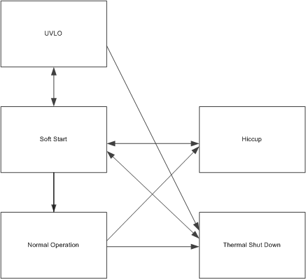 Figure 23. Mode Transition Diagram