SNVS363E August 2005 – November 2015 LM5026
PRODUCTION DATA.
- 1 Features
- 2 Applications
- 3 Description
- 4 Revision History
- 5 Pin Configuration and Functions
- 6 Specifications
-
7 Detailed Description
- 7.1 Overview
- 7.2 Functional Block Diagram
- 7.3
Feature Description
- 7.3.1 High Voltage Start-Up Regulator
- 7.3.2 Line Undervoltage Detector
- 7.3.3 PWM Outputs
- 7.3.4 Gate Driver Outputs
- 7.3.5 PWM Comparator/Slope Compensation
- 7.3.6 Maximum Duty Cycle Clamp
- 7.3.7 Soft-Start / Soft-Stop
- 7.3.8 Current Sense and Current Limit
- 7.3.9 Overload Protection Timer
- 7.3.10 Oscillator and Sync Capability
- 7.3.11 Thermal Protection
- 7.4 Device Functional Modes
-
8 Application and Implementation
- 8.1 Application Information
- 8.2 Typical Application
- 9 Power Supply Recommendations
- 10Layout
- 11Device and Documentation Support
- 12Mechanical, Packaging, and Orderable Information
Package Options
Mechanical Data (Package|Pins)
Thermal pad, mechanical data (Package|Pins)
Orderable Information
6 Specifications
6.1 Absolute Maximum Ratings
See (1)(2).| MIN | MAX | UNIT | ||
|---|---|---|---|---|
| VIN to GND | –0.3 | 105 | V | |
| VCC to GND | –0.3 | 16 | V | |
| CS to GND | –0.3 | 1 | V | |
| COMP input current | 10 | mA | ||
| All other inputs to GND | –0.3 | 7 | V | |
| Junction temperature | 150 | °C | ||
| Storage temperature, Tstg | –65 | 150 | °C | |
(1) Stresses beyond those listed under Absolute Maximum Ratings may cause permanent damage to the device. These are stress ratings only, which do not imply functional operation of the device at these or any other conditions beyond those indicated under Recommended Operating Conditions. Exposure to absolute-maximum-rated conditions for extended periods may affect device reliability.
(2) If Military/Aerospace specified devices are required, please contact the TI Sales Office/ Distributors for availability and specifications.
6.2 ESD Ratings
| VALUE | UNIT | |||
|---|---|---|---|---|
| V(ESD) | Electrostatic discharge | Human body model (HBM), per ANSI/ESDA/JEDEC JS-001(1)(3) | ±2000 | V |
| Charged-device model (CDM), per JEDEC specification JESD22-C101(2) | ±500 | |||
(1) JEDEC document JEP155 states that 500-V HBM allows safe manufacturing with a standard ESD control process. Manufacturing with less than 500-V HBM is possible with the necessary precautions. Pins listed as ±2000 V may actually have higher performance.
(2) JEDEC document JEP157 states that 250-V CDM allows safe manufacturing with a standard ESD control process.
(3) The human body model is a 100-pF capacitor discharged through a 1.5-kΩ resistor into each pin.
6.3 Recommended Operating Conditions
over operating free-air temperature range (unless otherwise noted)(1)| MIN | MAX | UNIT | ||
|---|---|---|---|---|
| VIN voltage | 13 | 100 | V | |
| External voltage applied to VCC | 8 | 15 | V | |
| Operating junction temperature | –40 | 125 | °C | |
(1) Absolute Maximum Ratings are limits beyond which damage to the device may occur. Operating Ratings are conditions under which operation of the device is intended to be functional. For specifications and test conditions, see the Electrical Characteristics.
6.4 Thermal Information
| THERMAL METRIC(1) | LM5026 | UNIT | ||
|---|---|---|---|---|
| NHQ (WSON) | PW (TSSOP) | |||
| 16 PINS | 16 PINS | |||
| RθJA | Junction-to-ambient thermal resistance | 29.9 | 98.6 | °C/W |
| RθJC(top) | Junction-to-case (top) thermal resistance | 25.8 | 27.6 | °C/W |
| RθJB | Junction-to-board thermal resistance | 9.2 | 44.1 | °C/W |
| ψJT | Junction-to-top characterization parameter | 0.2 | 1.2 | °C/W |
| ψJB | Junction-to-board characterization parameter | 9.5 | 43.3 | °C/W |
| RθJC(bot) | Junction-to-case (bottom) thermal resistance | 2.3 | — | °C/W |
(1) For more information about traditional and new thermal metrics, see the Semiconductor and IC Package Thermal Metrics application report, SPRA953.
6.5 Electrical Characteristics
Specification typical values are for TJ = 25°C unless otherwise noted. VIN = 48 V, VCC = 10 V, RT = 30.0 kΩ, Rset = 34.8 kΩ unless otherwise stated. Minimum and maximum specifications apply over full operating junction temperature range.(1)| PARAMETER | TEST CONDITIONS | MIN | TYP | MAX | UNIT | ||
|---|---|---|---|---|---|---|---|
| START-UP REGULATOR | |||||||
| VCC Reg | VCC regulation | No Load | TJ = 25°C | 7.6 | V | ||
| over full operating junction temperature range | 7.3 | 7.9 | |||||
| VCC current limit | See (2) | TJ = 25°C | 25 | mA | |||
| over full operating junction temperature range | 20 | ||||||
| I-VIN | Start-up regulator leakage (external VCC supply) | VIN = 100 V | TJ = 25°C | 165 | µA | ||
| over full operating junction temperature range | 500 | ||||||
| Shutdown current (Iin) | UVLO = 0 V | TJ = 25°C | 350 | µA | |||
| over full operating junction temperature range | 450 | ||||||
| VCC SUPPLY | |||||||
| VCC undervoltage lockout voltage (positive going Vcc) | TJ = 25°C | VCC Reg – 120 mV | V | ||||
| over full operating junction temperature range | VCC Reg – 220 mV | ||||||
| VCC undervoltage hysteresis | TJ = 25°C | 1.5 | V | ||||
| over full operating junction temperature range | 1 | 2 | |||||
| VCC supply current (ICC) | Cgate = 0, UVLO = 1.3 V, over full operating junction temperature range | 4.2 | mA | ||||
| REFERENCE SUPPLY | |||||||
| VREF | Ref voltage | IREF = 0 mA | TJ = 25°C | 5 | V | ||
| over full operating junction temperature range | 4.85 | 5.15 | |||||
| Ref voltage regulation | IREF = 0 to 10 mA | TJ = 25°C | 25 | mV | |||
| over full operating junction temperature range | 50 | ||||||
| Ref current limit | TJ = 25°C | 20 | mA | ||||
| over full operating junction temperature range | 10 | ||||||
| UVLO SHUTDOWN/STANDBY | |||||||
| Undervoltage shutdown threshold | TJ = 25°C | 0.4 | V | ||||
| over full operating junction temperature range | 0.3 | 0.5 | |||||
| Undervoltage shutdown hysteresis | 0.1 | V | |||||
| Undervoltage standby threshold | TJ = 25°C | 1.25 | V | ||||
| over full operating junction temperature range | 1.21 | 1.29 | |||||
| Undervoltage sandby hysteresis current source | TJ = 25°C | 20 | µA | ||||
| over full operating junction temperature range | 16 | 24 | |||||
| CURRENT LIMIT | |||||||
| Cycle-by-cycle threshold voltage | TJ = 25°C | 0.5 | V | ||||
| over full operating junction temperature range | 0.45 | 0.55 | |||||
| ILIM delay-to-output | CS step from 0 to 0.6 V Time to onset of OUT transition (90%) Cgate=0 | 40 | ns | ||||
| Leading edge blanking time | TJ = 25°C | 100 | ns | ||||
| over full operating junction temperature range | 70 | 130 | |||||
| CS sink impedance (clocked) | ICS = 10 mA | TJ = 25°C | 30 | Ω | |||
| over full operating junction temperature range | 65 | ||||||
| OVERCURRENT RESTART | |||||||
| Restart threshold | TJ = 25°C | 2.55 | V | ||||
| over full operating junction temperature range | 2.4 | 2.7 | |||||
| Fault-charging current | TJ = 25°C | 10 | µA | ||||
| over full operating junction temperature range | 7.5 | 12.5 | |||||
| Discharging current | TJ = 25°C | 10 | µA | ||||
| over full operating junction temperature range | 7.5 | 12.5 | |||||
| SOFT-START | |||||||
| Soft-start current source | TJ = 25°C | 50 | µA | ||||
| over full operating junction temperature range | 38 | 58 | |||||
| Soft-stop current sink | TJ = 25°C | 50 | |||||
| over full operating junction temperature range | 38 | 58 | |||||
| Soft-start current source following a restart event | TJ = 25°C | 1 | |||||
| over full operating junction temperature range | 0.6 | 1.3 | |||||
| OSCILLATOR | |||||||
| Frequency1 | RT = 30 kΩ | TJ = 25°C | 200 | kHz | |||
| over full operating junction temperature range | 180 | 220 | |||||
| Frequency2 | RT = 10 kΩ | TJ = 25°C | 590 | kHz | |||
| over full operating junction temperature range | 520 | 660 | |||||
| SYNC source current | 200 | µA | |||||
| SYNC sink impedance | Can sync up to 5 like controllers minimum | 100 | Ω | ||||
| Sync threshold (falling) | 1.4 | V | |||||
| Sync pulse width minimum | over full operating junction temperature range | 15 | ns | ||||
| PWM COMPARATOR | |||||||
| Delay-to-output | CS stepped, time to onset of OUT_A transition low | 40 | ns | ||||
| Mimimum duty cycle | ICOMP = 1 mA, over full operating junction temperature range | 0% | |||||
| Maximum duty cycle limit 1 | UVLO = 1.3 V, COMP = open, VDCL = 2.5 V | 80% | |||||
| Maximum duty cycle limit 2 | UVLO = 1.3 V, COMP = open, VDCL = VRT × 0.875 | 70% | |||||
| Maximum duty cycle limit 3 | UVLO = 2.92 V, COMP = open, VDCL = 2.5 V | 40% | |||||
| SS to PWM offset | 1.4 | V | |||||
| COMP input impedance | Small signal impedance | 1700 | Ω | ||||
| Slope compensation amplitude | Delta increase at PWM comparator to CS | TJ = 25°C | 90 | mV | |||
| over full operating junction temperature range | 75 | 115 | |||||
| OUTPUT SECTION | |||||||
| OUT_A high saturation | MOS Device at IOUT = –10 mA, |
TJ = 25°C | 5 | Ω | |||
| over full operating junction temperature range | 10 | ||||||
| OUTPUT_A peak current sink | Bipolar Device at VCC/2 | 3 | A | ||||
| OUT_A low saturation | MOS Device at IOUT = 10 mA, |
TJ = 25°C | 6 | Ω | |||
| over full operating junction temperature range | 9 | ||||||
| OUTPUT_A rise time | Cgate = 2.2 nF | 20 | ns | ||||
| OUTPUT_A fall time | Cgate = 2.2 nF | 15 | ns | ||||
| OUT_B high saturation | IOUT = –10 mA | TJ = 25°C | 10 | Ω | |||
| over full operating junction temperature range | 20 | ||||||
| OUT_B low saturation | IOUT = 10 mA | TJ = 25°C | 10 | Ω | |||
| over full operating junction temperature range | 20 | ||||||
| OUTPUT_B rise time | Cgate = 470 pF | 15 | ns | ||||
| OUTPUT_B fall time | Cgate = 470 pF | 15 | ns | ||||
| OUTPUT TIMING CONTROL | |||||||
| Overlap time | RSET = 34.8 kΩ connected to GND, 50% to 50% transitions | TJ = 25°C | 100 | ns | |||
| over full operating junction temperature range | 70 | 130 | |||||
| Deadtime | RSET = 30 kΩ connected to REF, 50% to 50% transitions | TJ = 25°C | 100 | ns | |||
| over full operating junction temperature range | 70 | 130 | |||||
| THERMAL SHUTDOWN | |||||||
| TSD | Thermal shutdown temp. | 150 | 165 | °C | |||
| Thermal shutdown hysteresis | 25 | °C | |||||
(1) Minimum and maximum limits are 100% production tested at 25ºC. Limits over the operating temperature range are specified through correlation using Statistical Quality Control (SQC) methods. Limits are used to calculate Average Outgoing Quality Level (AOQL). All electrical characteristics having room temperature limits are tested during production with TA = TJ = 25°C. All hot and cold limits are specified by correlating the electrical characteristics to process and temperature variations and applying statistical process control.
(2) Device thermal limitations may limit usable range.
6.6 Typical Characteristics
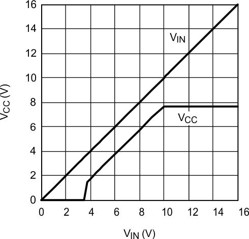 Figure 1. VCC Regulator Start-Up Characteristics, VCC vs VIN
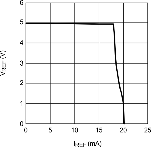 Figure 3. VREF vs IREF
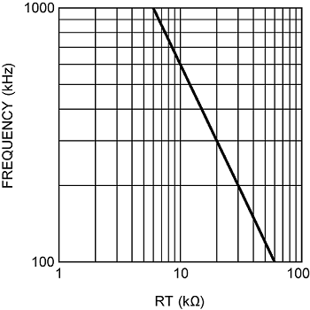 Figure 5. Oscillator Frequency vs RT
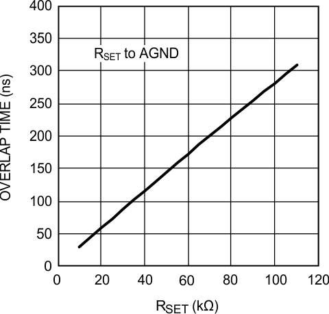 Figure 7. Overlap Time vs RSET
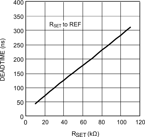 Figure 9. Deadtime vs RSET
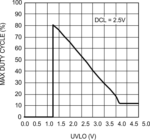 Figure 11. Max Duty Cycle vs UVLO
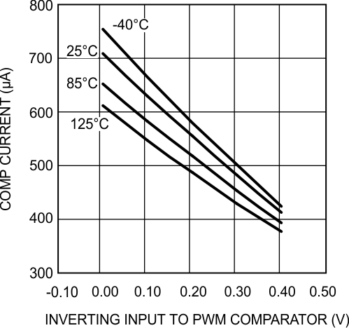 Figure 13. COMP Current vs INV PWM Comparator Voltage
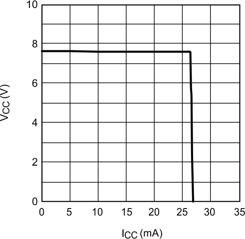 Figure 2. VCC vs ICC
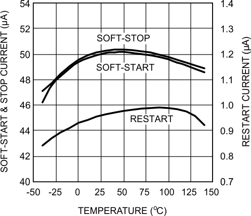 Figure 4. Soft-Start, Soft-Stop and Restart Current vs Temperature
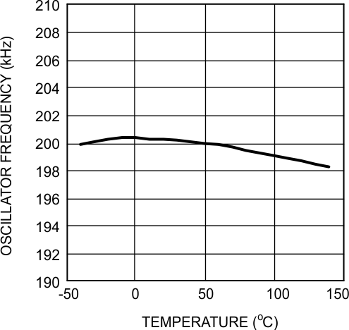 Figure 6. Oscillator Frequency vs Temperature
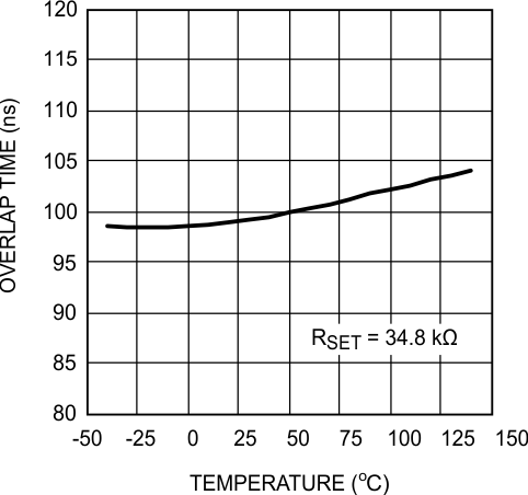 Figure 8. Overlap Time vs Temperature
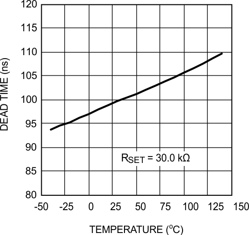 Figure 10. Deadtime vs Temperature
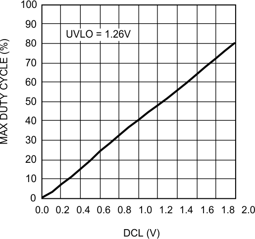 Figure 12. Max Duty Cycle vs DCL