SNVS699H February 2011 – January 2015 LM5045
PRODUCTION DATA.
- 1 Features
- 2 Applications
- 3 Description
- 4 Revision History
- 5 Pin Configuration and Functions
- 6 Specifications
-
7 Detailed Description
- 7.1 Overview
- 7.2 Functional Block Diagram
- 7.3
Feature Description
- 7.3.1 High-Voltage Start-Up Regulator
- 7.3.2 Line Undervoltage Detector
- 7.3.3 Overvoltage Protection
- 7.3.4 Reference
- 7.3.5 Oscillator, Sync Input
- 7.3.6 Cycle-by-Cycle Current Limit
- 7.3.7 Hiccup Mode
- 7.3.8 PWM Comparator
- 7.3.9 Ramp Pin
- 7.3.10 Slope Pin
- 7.3.11 Soft-Start
- 7.3.12 Gate Driver Outputs
- 7.3.13 Synchronous Rectifier Control Outputs (SR1 and SR2)
- 7.3.14 Soft-Start of the Synchronous Rectifiers
- 7.3.15 Prebias Startup
- 7.3.16 Soft-Stop
- 7.3.17 Soft-Stop Off
- 7.3.18 Thermal Protection
- 7.4 Device Functional Modes
- 8 Application and Implementation
- 9 Power Supply Recommendations
- 10Layout
- 11Device and Documentation Support
- 12Mechanical, Packaging, and Orderable Information
Package Options
Mechanical Data (Package|Pins)
Thermal pad, mechanical data (Package|Pins)
- PWP|28
Orderable Information
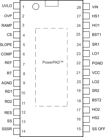
5 Pin Configuration and Functions
PWP Package
28-Pin HTSSOP With PowerPAD™
Top View
RSG Package
28-Pin WQFN, 5 mm × 5 mm
Top View
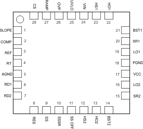
Pin Functions
| PIN | I/O | DESCRIPTION | APPLICATION INFORMATION | ||
|---|---|---|---|---|---|
| NAME | HTSSOP | WQFN | |||
| AGND | 9 | 5 | O | Analog Ground | Connect directly to the Power Ground. |
| BST1 | 25 | 21 | I | Gate Drive Bootstrap | Bootstrap capacitors connected between BST1, 2 and SW1, 2 provide bias supply for the high side HO1, 2 gate drivers. External diodes are required between VCC and BST1, 2 to charge the bootstrap capacitors when SW1, 2 are low. |
| BST2 | 18 | 14 | |||
| COMP | 6 | 2 | I | Input to the Pulse Width Modulator | An external opto-coupler connected to the COMP pin sources current into an internal NPN current mirror. The PWM duty cycle is at maximum with zero input current, while 1 mA reduces the duty cycle to zero. The current mirror improves the frequency response by reducing the AC voltage across the opto-coupler. |
| CS | 4 | 28 | I | Current Sense Input | If CS exceeds 750 mV the PWM output pulse will be terminated, entering cycle-by-cycle current limit. An internal switch holds CS low for 40 nS after either output switches high to blank leading edge transients. |
| HO1 | 26 | 22 | O | High Side Output Driver | High side PWM outputs capable of driving the upper MOSFET of the bridge with 1.5-A peak source and 2-A peak sink current. |
| HO2 | 17 | 13 | |||
| HS1 | 27 | 23 | I | Switch Node | Common connection of the high side FET source, low side FET drain and transformer primary winding. |
| HS2 | 16 | 12 | |||
| LO1 | 23 | 19 | O | Low Side Output Driver | Alternating output of the PWM gate driver. Capable of 1.5-A peak source and 2-A peak sink current. |
| LO2 | 20 | 16 | |||
| OVP/OTP | 2 | 26 | I | Overvoltage Protection | An external voltage divider from the input power supply sets the shutdown level during an over-voltage condition. Alternatively, an external NTC thermistor voltage divider can be used to set the shutdown temperature. The threshold is 1.25 V. Hysteresis is set by an internal current that sources 20 µA of current into the external resistor divider. |
| PGND | 22 | 18 | O | Power Ground | Connect directly to Analog Ground |
| RAMP | 3 | 27 | I | Input to PWM Comparator | Modulation ramp for the PWM comparator. This ramp can be a signal representative of the primary current (current mode) or proportional to the input voltage (feed-forward voltage mode). This pin is reset to GND at the end of every cycle. |
| RD1 | 10 | 6 | I | Synchronous Rectifier Leading Edge Delay | The resistance connected between RD1 and AGND sets the delay from the falling edge of SR1 or SR2 and the rising edge of HO2/LO1 or HO1/LO2, respectively. |
| RD2 | 11 | 7 | I | Synchronous Rectifier Trailing Edge Delay | The resistance connected between RD2 and AGND sets the delay from the falling edge of HO1/LO2 or HO2/LO1 and the rising edge of SR2 or SR1, respectively. |
| REF | 7 | 3 | O | Output of a 5V reference | Maximum output current is 15 mA. Locally decouple with a 0.1-µF capacitor. |
| RES | 12 | 8 | I | Restart Timer | Whenever the CS pin exceeds the 750-mV cycle-cycle current limit threshold, 30-µA current is sourced into the RES capacitor for the remainder of the PWM cycle. If the RES capacitor voltage reaches 1.0 V, the SS capacitor is discharged to disable the HO1, HO2, LO1, LO2 and SR1, SR2 outputs. The SS pin is held low until the voltage on the RES capacitor has been ramped between 2-V and 4-V eight times by 10-µA charge and 5-µA discharge currents. After the delay sequence, the SS capacitor is released to initiate a normal start-up sequence. |
| RT/SYNC | 8 | 4 | O | Oscillator Frequency Control and Frequency Synchronization | The resistance connected between RT and AGND sets the oscillator frequency. Synchronization is achieved by AC coupling a pulse to the RT/SYNC pin that raises the voltage at least 1.5 V above the 2-V nominal bias level. |
| SLOPE | 5 | 1 | O | Slope Compensation Current | A ramping current source from 0 to 100 µA is provided for slope compensation in current mode control. This pin can be connected through an appropriate resistor to the CS pin to provide slope compensation. If slope compensation is not required, SLOPE must be tied to ground. |
| SR1 | 24 | 20 | O | Synchronous Rectifier Driver | Control output for synchronous rectifier gate. Capable of peak sourcing 100 mA and sinking 400 mA. |
| SR2 | 19 | 15 | O | Synchronous Rectifier Driver | Control output for synchronous rectifier gate. Capable of peak sourcing 100 mA and sinking 400 mA. |
| SS | 13 | 9 | I | Soft-Start Input | An internal 20-µA current source charges the SS pin during start-up. The input to the PWM comparator gradually rises as the SS capacitor charges to steadily increase the PWM duty cycle. Pulling the SS pin to a voltage below 20 0mV stops PWM pulses at HO1, 2 and LO1, 2 and turns off the synchronous rectifier FETs to a low state. |
| SSOFF | 15 | 11 | I | Soft-Stop Disable | When SS OFF pin is connected to the AGND, the LM5045 soft-stops in the event of a VIN UVLO and Hiccup mode current limit condition. If the SSOFF pin is connected to REF pin, the controller hard-stops on any fault condition. Refer to Table 1 for more details. |
| SSSR | 14 | 10 | I | Secondary Side Soft-Start | An external capacitor and an internal 20-µA current source set the soft-start ramp for the synchronous rectifiers. The SSSR capacitor charge-up is enabled after the first output pulse and SS > 2 V and Icomp < 800 µA |
| UVLO | 1 | 25 | I | Line Undervoltage Lockout | An external voltage divider from the power source sets the shutdown and standby comparator levels. When UVLO reaches the 0.4-V threshold the VCC and REF regulators are enabled. At the 1.25-V threshold, the SS pin is released and the controller enters the active mode. Hysteresis is set by an internal current sink that pulls 20 µA from the external resistor divider. |
| VCC | 21 | 17 | I | Output of Start-Up Regulator | The output voltage of the start-up regulator is initially regulated to 9.5 V. Once the secondary side soft-start (SSSR pin) reaches 1 V, the VCC output is reduced to 7.7 V. If an auxiliary winding raises the voltage on this pin above the regulation set-point, the internal start-up regulator will shutdown, thus reducing the IC power dissipation. |
| VIN | 28 | 24 | I | Input Power Source | Input to the Start-up Regulator. Operating input range is 14 V to 100 V. For power sources outside of this range, the LM5045 can be biased directly at VCC by an external regulator. |