SNVS333F November 2004 – September 2016 LM5107
PRODUCTION DATA.
- 1 Features
- 2 Applications
- 3 Description
- 4 Revision History
- 5 Pin Configuration and Functions
- 6 Specifications
- 7 Detailed Description
- 8 Application and Implementation
- 9 Power Supply Recommendations
- 10Layout
- 11Device and Documentation Support
- 12Mechanical, Packaging, and Orderable Information
Package Options
Mechanical Data (Package|Pins)
Thermal pad, mechanical data (Package|Pins)
Orderable Information
7 Detailed Description
7.1 Overview
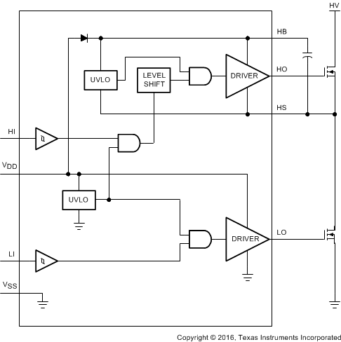
The LM5107 is designed to drive both the high-side and the low-side N-channel FETs in a synchronous buck or a half-bridge configuration. The outputs are independently controlled with TTL input thresholds. The floating high-side driver is capable of working with supply voltages up to 100 V. An integrated high voltage diode is provided to charge high side gate drive bootstrap capacitor. A robust level shifter operates at high speed while consuming low power and providing clean level transitions from the control logic to the high side gate driver. Undervoltage lockout is provided on both the low side and the high side power rails.
7.2 Functional Block Diagram

7.3 Feature Description
7.3.1 Start-up and UVLO
Both high and low-side drivers include under voltage lockout (UVLO) protection circuitry which monitors the supply voltage (VDD) and bootstrap capacitor voltage (VHB–HS) independently. The UVLO circuit inhibits each driver until sufficient supply voltage is available to turn on the external MOSFETs, and the built-in UVLO hysteresis prevents chattering during supply voltage transitions. When the supply voltage is applied to the VDD pin of the LM5107, the outputs of the low-side and high-side are held low until VDD exceeds the UVLO threshold, typically about 6.9 V. Any UVLO condition on the bootstrap capacitor will disable only the high-side output (HO).
7.3.2 Level Shift
The level shift circuit is the interface from the high-side input to the high-side driver stage which is referenced to the switch node (HS). The level shift allows control of the HO output referenced to the HS pin and provides excellent delay matching with the low-side driver.
7.3.3 Bootstrap Diode
The bootstrap diode necessary to generate the high-side bias is included in the LM5107. The diode anode is connected to VDD and cathode connected to VHB. With the VHB capacitor connected to HB and the HS pins, the VHB capacitor charge is refreshed every switching cycle when HS transitions to ground. The boot diode provides fast recovery times, low diode resistance, and voltage rating margin to allow for efficient and reliable operation.
7.3.4 Output Stages
The output stages are the interface to the power MOSFETs in the power train. High slew rate, low resistance, and high peak current capability of both output drivers allow for efficient switching of the power MOSFETs. The low-side output stage is referenced from VDD to VSS and the high-side is referenced from VHB to VHS.
7.4 Device Functional Modes
The device operates in normal mode and UVLO mode. See Start-up and UVLO for more information on UVLO operation mode. In normal mode, the output stage is dependent on the states of the HI and LI pins.