SNVS790F January 2012 – November 2015 LM5114
PRODUCTION DATA.
- 1 Features
- 2 Applications
- 3 Description
- 4 Revision History
- 5 Device Comparison Table
- 6 Pin Configuration and Functions
- 7 Specifications
- 8 Detailed Description
- 9 Application and Implementation
- 10Power Supply Recommendations
- 11Layout
- 12Device and Documentation Support
- 13Mechanical, Packaging, and Orderable Information
Package Options
Mechanical Data (Package|Pins)
Thermal pad, mechanical data (Package|Pins)
Orderable Information
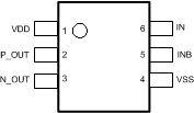
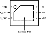
6 Pin Configuration and Functions
DBV Package
6-Pin SOT-23
Top View

NGG Package
6-Pin WSON
Top View

Pin Functions
| PIN | I/O | DESCRIPTION | ||
|---|---|---|---|---|
| NAME | SOT-23 | WSON | ||
| IN | 6 | 6 | I | Noninverting logic input Connect to VDD when not used. |
| INB | 5 | 5 | I | Inverting logic input Connect to VSS when not used. |
| N_OUT | 3 | 3 | O | Sink-current output Connect to the gate of the MOSFET with a short, low inductance path. A gate resistor can be used to adjust the turnoff speed. |
| P_OUT | 2 | 2 | O | Source-current output Connect to the gate of the MOSFET with a short, low inductance path. A gate resistor can be used to adjust the turnon speed. |
| VDD | 1 | 1 | — | Gate drive supply Locally decouple to VSS using low ESR/ESL capacitor located as close as possible to the IC. |
| VSS | 4 | 4 | — | Ground All signals are referenced to this ground. |
| EP | — | ✓ | — | It is recommended that the exposed pad on the bottom of the package is soldered to ground plane on the PC board to aid thermal dissipation. |