SNVS698F April 2011 – August 2015 LM5117 , LM5117-Q1
PRODUCTION DATA.
- 1 Features
- 2 Applications
- 3 Description
- 4 Revision History
- 5 Pin Configuration and Functions
- 6 Specifications
-
7 Detailed Description
- 7.1 Overview
- 7.2 Functional Block Diagram
- 7.3
Feature Description
- 7.3.1 High Voltage Start-up Regulator and VCC Disable
- 7.3.2 UVLO
- 7.3.3 Oscillator and Sync Capability
- 7.3.4 Ramp Generator and Emulated Current Sense
- 7.3.5 Error Amplifier and PWM Comparator
- 7.3.6 Soft-Start
- 7.3.7 Cycle-by-Cycle Current Limit
- 7.3.8 Hiccup Mode Current Limiting
- 7.3.9 HO and LO Drivers
- 7.3.10 Current Monitor
- 7.3.11 Maximum Duty Cycle
- 7.3.12 Thermal Protection
- 7.4 Device Functional Modes
-
8 Application and Implementation
- 8.1 Application Information
- 8.2 Typical Applications
- 8.3
Detailed Design Procedure
- 8.3.1 Feedback Compensation
- 8.3.2 Sub-Harmonic Oscillation
- 8.3.3 Design Requirements
- 8.3.4 Timing Resistor RT
- 8.3.5 Output Inductor LO
- 8.3.6 Diode Emulation Function
- 8.3.7 Current Sense Resistor RS
- 8.3.8 Current Sense Filter RCS and CCS
- 8.3.9 Ramp Resistor RRAMP and Ramp Capacitor CRAMP
- 8.3.10 UVLO Divider RUV2, RUV1 and CFT
- 8.3.11 VCC Disable and External VCC Supply
- 8.3.12 Power Switches QH and QL
- 8.3.13 Snubber Components RSNB and CSNB
- 8.3.14 Bootstrap Capacitor CHB and Bootstrap Diode DHB
- 8.3.15 VCC Capacitor CVCC
- 8.3.16 Output Capacitor CO
- 8.3.17 Input Capacitor CIN
- 8.3.18 VIN Filter RVIN, CVIN
- 8.3.19 Soft-Start Capacitor CSS
- 8.3.20 Restart Capacitor CRES
- 8.3.21 Output Voltage Divider RFB2 and RFB1
- 8.3.22 Loop Compensation Components CCOMP, RCOMP and CHF
- 8.4 Application Curves
- 9 Power Supply Recommendations
- 10Layout
- 11Device and Documentation Support
- 12Mechanical, Packaging, and Orderable Information
Package Options
Mechanical Data (Package|Pins)
Thermal pad, mechanical data (Package|Pins)
Orderable Information
8 Application and Implementation
NOTE
Information in the following applications sections is not part of the TI component specification, and TI does not warrant its accuracy or completeness. TI’s customers are responsible for determining suitability of components for their purposes. Customers should validate and test their design implementation to confirm system functionality.
8.1 Application Information
The LM5117 is a step-down dc-dc controller. The device is typically used to convert a higher dc-dc voltage to a lower dc voltage. Use the following design procedure to select component values. Alternately, use the WEBENCH® software to generate a complete design. The WEBENCH software uses an iterative design procedure and assesses a comprehensive database of components when generating a design.
8.2 Typical Applications
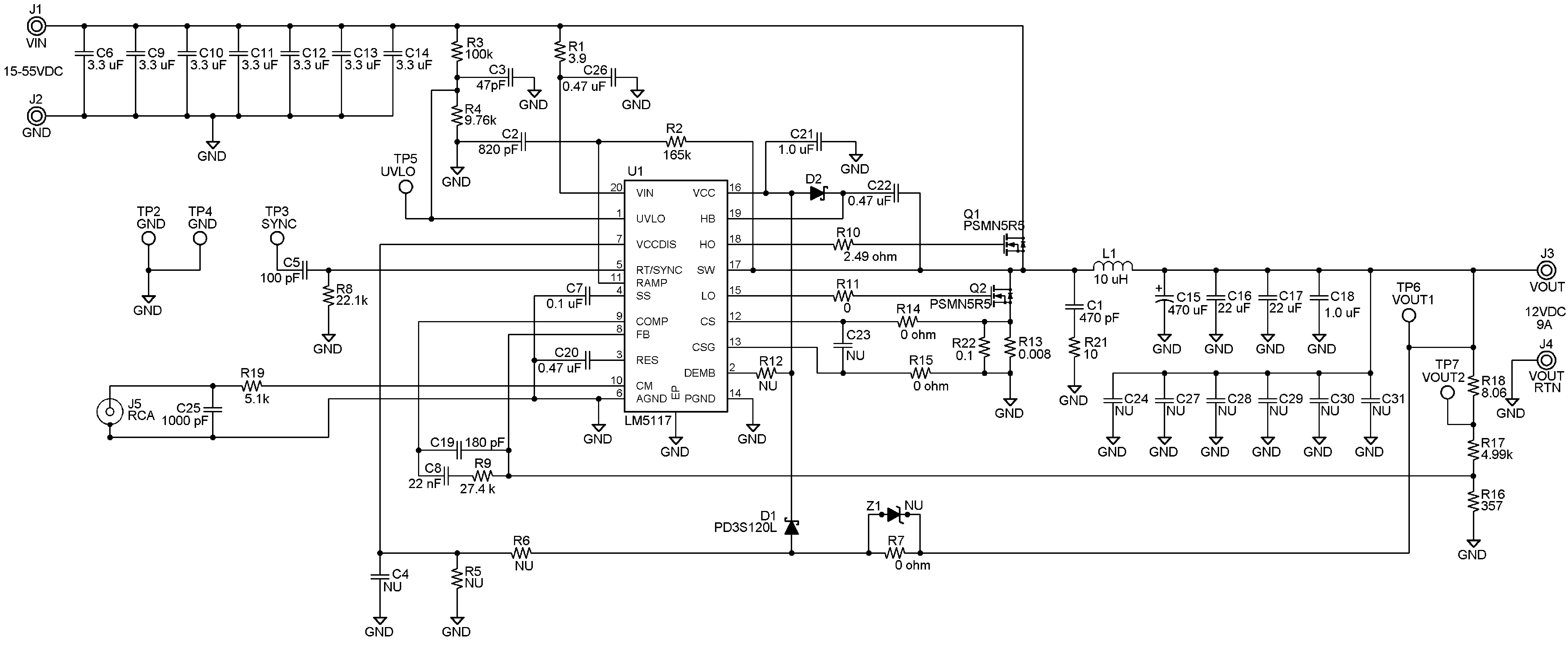 Figure 29. 12 V, 9 A Typical Application Schematic
8.3 Detailed Design Procedure
8.3.1 Feedback Compensation
Open loop response of the regulator is defined as the product of modulator transfer function and feedback transfer function. When plotted on a dB scale, the open loop gain is shown as the sum of modulator gain and feedback gain.
The modulator transfer function includes a power stage transfer function with an embedded current loop and can be simplified as one pole and one zero system as shown in Equation 15.


If the ESR of COUT (RESR) is very small, the modulator transfer function can be further simplified to a one pole system and the voltage loop can be closed with only two loop compensation components, RCOMP and CCOMP, leaving a single pole response at the crossover frequency. A single pole response at the crossover frequency yields a very stable loop with 90 degrees of phase margin.
The feedback transfer function includes the feedback resistor divider and loop compensation of the error amplifier. RCOMP, CCOMP and optional CHF configure the error amplifier gain and phase characteristics and create a pole at origin, a low frequency zero and a high frequency pole. This is shown mathematically in Equation 16.


The pole at the origin minimizes output steady state error. The low frequency zero should be placed to cancel the load pole of the modulator. The high frequency pole can be used to cancel the zero created by the output capacitor ESR or to decrease noise susceptibility of the error amplifier. By placing the low frequency zero an order of magnitude less than the crossover frequency, the maximum amount of phase boost can be achieved at the crossover frequency. The high frequency pole should be placed well beyond the crossover frequency since the addition of CHF adds a pole in the feedback transfer function.
The crossover frequency (loop bandwidth) is usually selected between one twentieth and one fifth of the fSW. In a simplified formula, the crossover frequency can be defined as:

For higher crossover frequency, RCOMP can be increased, while proportionally decreasing CCOMP. Conversely, decreasing RCOMP while proportionally increasing CCOMP, results in lower bandwidth while keeping the same zero frequency in the feedback transfer function.
The sampled gain inductor pole is inversely proportional to the K factor, which is defined as:

The maximum achievable loop bandwidth, in fact, is limited by this sampled gain inductor pole. In traditional current mode control, the maximum achievable loop bandwidth varies with input voltage. With the LM5117’s unique slope compensation scheme, the sampled gain inductor pole is independent of changes to the input voltage. This frees the user from additional concerns in wide varying input range applications and is an advantage of the LM5117.
If the sampled gain inductor pole or the ESR zero is close to the crossover frequency, it is recommended that the comprehensive formulas in Table 1 be used and the stability should be checked by a network analyzer. The modulator transfer function can be measured and the feedback transfer function can be configured for the desired open loop transfer function. If a network analyzer is not available, step load transient tests can be performed to verify acceptable performance. The step load goal is minimum overshoot/undershoot with a damped response.
8.3.2 Sub-Harmonic Oscillation
Peak current mode regulators can exhibit unstable behavior when operating above 50% duty cycle. This behavior is known as sub-harmonic oscillation and is characterized by alternating wide and narrow pulses at the SW pin. Sub-harmonic oscillation can be prevented by adding an additional voltage ramp (slope compensation) on top of the sensed inductor current shown in Figure 20. By choosing K≥1, the regulator will not be subject to sub-harmonic oscillation caused by a varying input voltage.
In time-domain analysis, the steady-state inductor current starts and ends at the same value during one clock cycle. If the magnitude of the end-of-cycle current error, dI1, caused by an initial perturbation, dI0, is less than the magnitude of dI0 or dI1/dI0 > -1, the perturbation naturally disappears after a few cycles. When dI1/dI0 < -1, the initial perturbation does not disappear, resulting in sub-harmonic oscillation in steady-state operation.
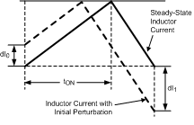 Figure 30. Effect of Initial Perturbation when dl1/dl0 < -1
dI1/dI0 can be calculated by:

The relationship between dI1/dI0 and K factor is illustrated graphically in Figure 31.
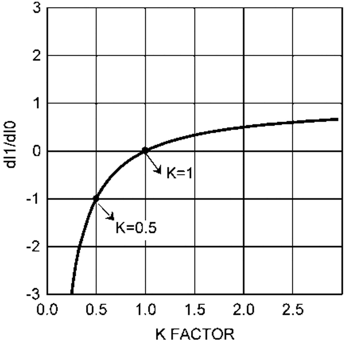 Figure 31. dl1/dl0 vs K Factor
The minimum value of K is 0.5. When K<0.5, the amplitude of dI1 is greater than the amplitude of dI0 and any initial perturbation results in sub-harmonic oscillation. If K=1, any initial perturbation will be removed in one switching cycle. This is known as one-cycle damping. When -1<dl1/dl0<0, any initial perturbation will be under-damped. Any perturbation will be over-damped when 0<dl1/dl0<1.
In the frequency-domain, Q, the quality factor of the sampling gain term in the modulator transfer function, is used to predict the tendency for sub-harmonic oscillation, which is defined as:

The relationship between Q and K factor is illustrated graphically in Figure 32.
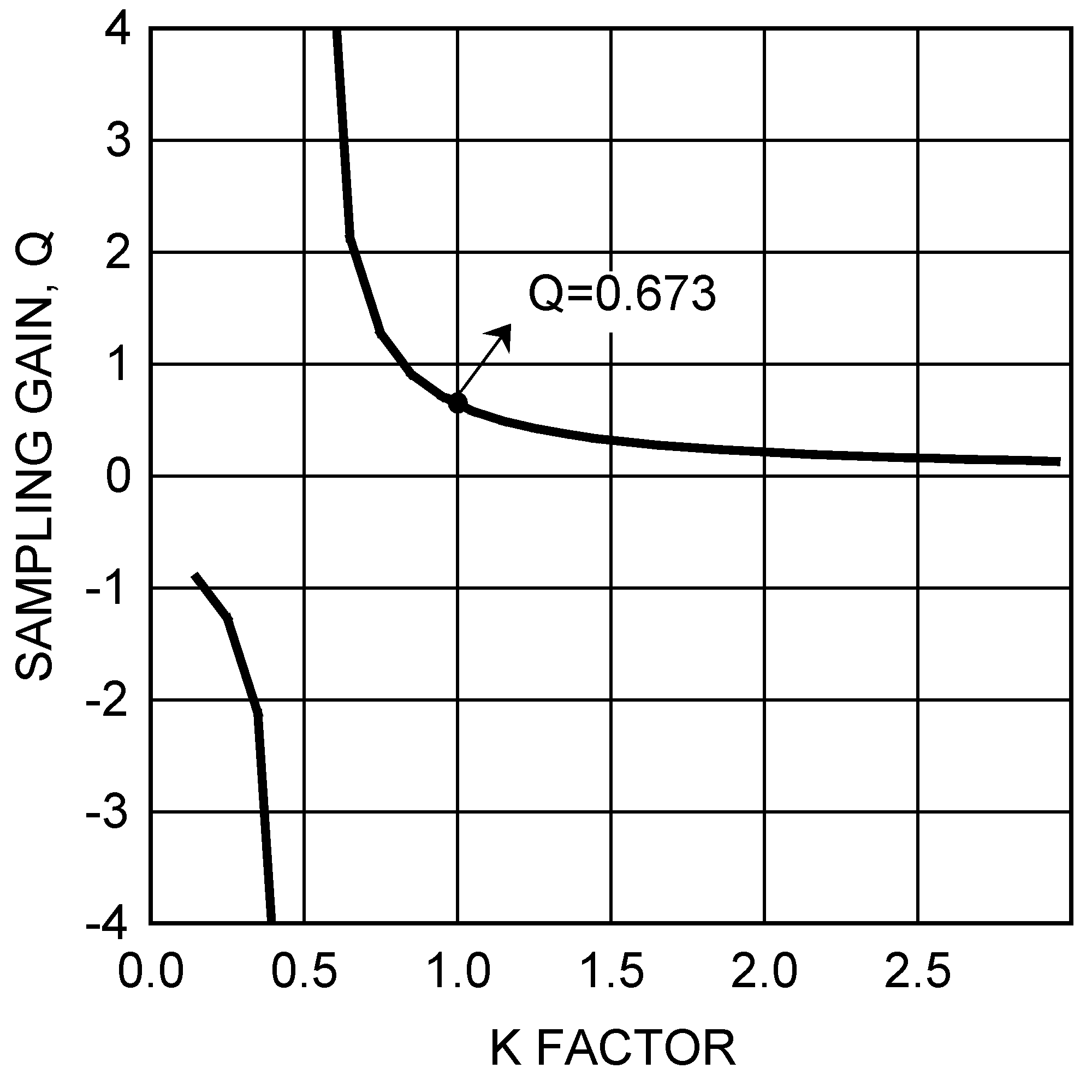 Figure 32. Sampling gain Q vs K Factor
The minimum value of K is 0.5 again. This is the same as time domain analysis result. When K<0.5, the regulator is unstable. High gain peaking at 0.5 results in sub-harmonic oscillation at FSW/2. When K=1, one-cycle damping is realized. Q is equal to 0.673 at this point. A higher K factor may introduce additional phase shift by moving the sampled gain inductor pole closer to the crossover frequency, but will help reduce noise sensitivity in the current loop. The maximum allowable value of K factor can be calculated by the Maximum Crossover Frequency equation in Table 1.
8.3.3 Design Requirements
| DESIGN PARAMETER | EXAMPLE VALUE |
|---|---|
| Output voltage | 12 V |
| Full load current, IOUT | 9 A |
| Minimum input voltage, VIN(MIN) | 15 V |
| Maximum input voltage, VIN(MAX) | 55 V |
| Switching frequency, ƒSW | 230 kHz |
| Diode emulation | yes |
| External VCC supply | yes |
8.3.4 Timing Resistor RT
Generally, higher frequency applications are smaller but have higher losses. Operation at 230 kHz was selected for this example as a reasonable compromise between small size and high efficiency. The value of RT for 230 kHz switching frequency can be calculated from Equation 3 as follows:

A standard value of 22.1 kΩ was chosen for RT.
8.3.5 Output Inductor LO
The maximum inductor ripple current occurs at the maximum input voltage. Typically, 20% to 40% of the full load current is a good compromise between core loss and copper loss of the inductor. Higher ripple current allows for a smaller inductor size, but places more of a burden on the output capacitor to smooth the ripple voltage on the output. For this example, a ripple current of 40% of 9 A was chosen. Knowing the switching frequency, maximum ripple current, maximum input voltage and the nominal output voltage, the inductor value can be calculated as follows:

The closest standard value of 10 μH was chosen for LO. Using the value of 10 μH for LO, calculate IPP again. This step is necessary if the chosen value of LO differs significantly from the calculated value.
From Equation 11,

At the minimum input voltage, this value is 1.04 A.
8.3.6 Diode Emulation Function
The DEMB pin is left floating since this example uses diode emulation to reduce the power loss under no load or light load conditions.
8.3.7 Current Sense Resistor RS
The performance of the converter will vary depending on the K value. For this example, K = 1 was chosen to control sub-harmonic oscillation and achieve one-cycle damping. The maximum output current capability (IOUT(MAX)) should be 20~50% higher than the required output current, to account for tolerances and ripple current. For this example, 130% of 9 A was chosen. The current sense resistor value can be calculated from Equation 9 and Equation 10 as follows:


A value of 7.41 mΩ was realized for RS by placing an additional 0.1-Ω sense resistor in parallel with 8 mΩ. The sense resistor must be rated to handle the power dissipation at maximum input voltage when current flows through the low-side NMOS for the majority of the PWM cycle. The maximum power dissipation of RS can be calculated as:


The worst case peak inductor current under the output short condition can be calculated from Equation 12 as follows:

where
- tON(MIN) is normally 100ns
8.3.8 Current Sense Filter RCS and CCS
The LM5117 itself is not affected by the large leading edge spike because it samples valley current just prior to the onset of the high-side switch. A current sense filter is used to minimize a noise injection from any external noise sources. In general, a current sense filter is not necessary. In this example, a current sense filter is not used
Adding RCS resistor changes the current sense amplifier gain which is defined as AS=10 k / (1 k+RCS). A small value of RCS resistor below 100 Ω is recommended to minimize the gain change which is caused by the temperature coefficient difference between internal and external resistors.
8.3.9 Ramp Resistor RRAMP and Ramp Capacitor CRAMP
The positive slope of the inductor current ramp signal is emulated by RRAMP and CRAMP. For this example, the value of CRAMP was set at the standard capacitor value of 820 pF. With the inductor, sense resistor and the K factor selected, the value of RRAMP can be calculated from Equation 4 as follows:


The standard value of 165 kΩ was selected for RRAMP.
8.3.10 UVLO Divider RUV2, RUV1 and CFT
The desired startup voltage and the hysteresis are set by the voltage divider RUV1 and RUV2. Capacitor CFT provides filtering for the divider. For this design, the startup voltage was set to 14 V, 1 V below VIN(MIN). VHYS was set to 2 V. The value of RUV1, RUV2 can be calculated from Equation 1 and Equation 2 as follows:


The standard value of 100 kΩ was selected for RUV2. RUV1 was selected to be 9.76 kΩ. A value of 47 pF was chosen for CFT.
8.3.11 VCC Disable and External VCC Supply
The 12-V output voltage allows the external VCC supply configuration as shown in Figure 16. In this example, VCCDIS can be left floating since VOUT is higher than VCC regulator set-point level.
8.3.12 Power Switches QH and QL
Selection of the power NMOS devices is governed by the same trade-offs as switching frequency. Breaking down the losses in the high-side and low-side NMOS devices is one way to compare the relative efficiencies of different devices. Losses in the power NMOS devices can be broken down into conduction loss, gate charging loss, and switching loss.
Conduction loss PDC is approximately:


where
- D is the duty cycle
- the factor of 1.3 accounts for the increase in the NMOS device on-resistance due to heating
Alternatively, the factor of 1.3 can be eliminated and the high temperature on-resistance of the NMOS device can be estimated using the RDS(ON) vs Temperature curves in the MOSFET datasheet.
Gate charging loss (PGC) results from the current driving the gate capacitance of the power NMOS devices and is approximated as:

Qg refers to the total gate charge of an individual NMOS device, and ‘n’ is the number of NMOS devices. Gate charge loss differs from conduction and switching losses in that the actual dissipation occurs in the controller IC. Switching loss (PSW) occurs during the brief transition period as the high-side NMOS device turns on and off. During the transition period both current and voltage are present in the channel of the NMOS device. The switching loss can be approximated as:

tR and tF are the rise and fall times of the high-side NMOS device. The rise and fall times are usually mentioned in the MOSFET datasheet or can be empirically observed with an oscilloscope. Switching loss is calculated for the high-side NMOS device only. Switching loss in the low-side NMOS device is negligible because the body diode of the low-side NMOS device turns on before and after the low-side NMOS device switches. For this example, the maximum drain-to-source voltage applied to either NMOS device is 55 V. The selected NMOS devices must be able to withstand 55 V plus any ringing from drain to source and must be able to handle at least the VCC voltage plus any ringing from gate to source.
8.3.13 Snubber Components RSNB and CSNB
A resistor-capacitor snubber network across the low-side NMOS device reduces ringing and spikes at the switching node. Excessive ringing and spikes can cause erratic operation and can couple noise to the output voltage. Selecting the values for the snubber is best accomplished through empirical methods. First, make sure the lead lengths for the snubber connections are very short. Start with a resistor value between 5 and 50 Ω. Increasing the value of the snubber capacitor results in more damping, but higher snubber losses. Select a minimum value for the snubber capacitor that provides adequate damping of the spikes on the switch waveform at heavy load. A snubber may not be necessary with an optimized layout.
8.3.14 Bootstrap Capacitor CHB and Bootstrap Diode DHB
The bootstrap capacitor between the HB and SW pin supplies the gate current to charge the high-side NMOS device gate during each cycle’s turn-on and also supplies recovery charge for the bootstrap diode. These current peaks can be several amperes. The recommended value of the bootstrap capacitor is at least 0.1 μF. CHB should be a good quality, low ESR, ceramic capacitor located at the pins of the IC to minimize potentially damaging voltage transients caused by trace inductance. The absolute minimum value for the bootstrap capacitor is calculated as:

where
- Qg is the high-side NMOS gate charge
- ΔVHB is the tolerable voltage droop on CHB, which is typically less than 5% of VCC or 0.15 V conservatively
A value of 0.47 μF was selected for this design.
8.3.15 VCC Capacitor CVCC
The primary purpose of the VCC capacitor (CVCC) is to supply the peak transient currents of the LO driver and bootstrap diode as well as provide stability for the VCC regulator. These peak currents can be several amperes. The recommended value of CVCC should be no smaller than 0.47μF, and should be a good quality, low ESR, ceramic capacitor. CVCC should be placed at the pins of the IC to minimize potentially damaging voltage transients caused by trace inductance. A value of 1 μF was selected for this design.
8.3.16 Output Capacitor CO
The output capacitors smooth the output voltage ripple caused by inductor ripple current and provide a source of charge during transient loading conditions. For this design example, a 470-μF electrolytic capacitor with maximum 20mΩ ESR was selected as the main output capacitor. The fundamental component of the output ripple voltage with maximum ESR is approximated as:


Additional low ERS / ESL ceramic capacitors can be placed in parallel with the main output capacitor to further reduce the output voltage ripple and spikes. In this example, two 22μF capacitors were added.
8.3.17 Input Capacitor CIN
The regulator input supply voltage typically has high source impedance at the switching frequency. Good quality input capacitors are necessary to limit the ripple voltage at the VIN pin while supplying most of the switch current during the on-time. When the high-side NMOS device turns on, the current into the device steps to the valley of the inductor current waveform, ramps up to the peak value, and then drops to the zero at turnoff. The input capacitor should be selected for RMS current rating and minimum ripple voltage. A good approximation for the required ripple current rating necessary is IRMS > IOUT / 2.
In this example, seven 3.3μF ceramic capacitors were used. With ceramic capacitors, the input ripple voltage will be triangular. The input ripple voltage can be approximated as:

Capacitors connected in parallel should be evaluated for RMS current rating. The current will split between the input capacitors based on the relative impedance of the capacitors at the switching frequency.
8.3.18 VIN Filter RVIN, CVIN
An R-C filter (RVIN, CVIN) on VIN is optional. The filter helps to prevent faults caused by high frequency switching noise injection into the VIN pin. A 0.47-μF ceramic capacitor is used for CVIN in the example. RVIN is selected to be 3.9 Ω.
8.3.19 Soft-Start Capacitor CSS
The capacitor at the SS pin (CSS) determines the soft-start time (tSS), which is the time for the output voltage to reach the final regulated value. The tSS for a given CSS can be calculated from Equation 8 as follows:

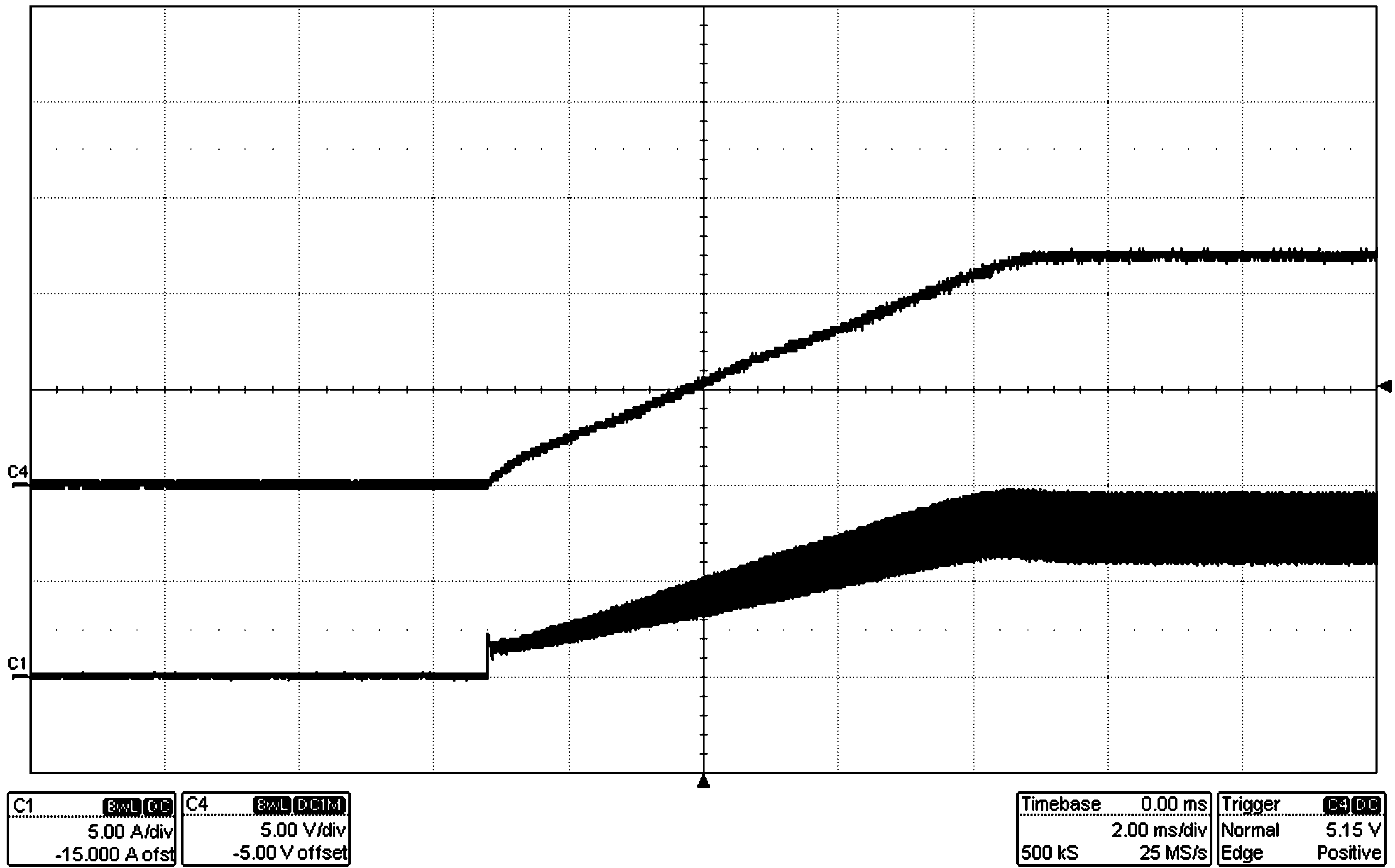
For this example, a value of 0.1 μF was chosen for a soft-start time of 8 ms.
8.3.20 Restart Capacitor CRES
The capacitor at the RES pin (CRES) determines tRES, which is the time the LM5117 remains off before a restart attempt is made in hiccup mode current limiting. tRES for a given CRES can be calculated from Equation 13 as follows:

For this example, a value of 0.47 μF was chosen for a restart time of 59 ms.
8.3.21 Output Voltage Divider RFB2 and RFB1
RFB1 and RFB2 set the output voltage level. The ratio of these resistors is calculated as:

The ratio between RCOMP and RFB2 determines the mid-band gain, AFB_MID. A larger value for RFB2 may require a corresponding larger value for RCOMP. RFB2 should be large enough to keep the total divider power dissipation small. 4.99 kΩ was chosen for RFB2 in this example, which results in a RFB1 value of 357 Ω for 12-V output.
8.3.22 Loop Compensation Components CCOMP, RCOMP and CHF
RCOMP, CCOMP and CHF configure the error amplifier gain and phase characteristics to produce a stable voltage loop. For a quick start, follow the 4 steps listed below.
STEP1: Select fCROSS
By selecting one tenth of the switching frequency, fCROSS is calculated as follows:

STEP2: Determine required RCOMP
Knowing fCROSS, RCOMP is calculated as follows:


The standard value of 27.4kΩ was selected for RCOMP
STEP3: Determine CCOMP to cancel load pole
Knowing RCOMP, CCOMP is calculated as follows:

The standard value of 22nF was selected for CCOMP
STEP4: Determine CHF to cancel ESR zero
Knowing RCOMP and CCOMP, CHF is calculated as follows:


Half of the maximum ESR is assumed as a typical ESR. The standard value of 180pF was selected for CHF.
Table 1. LM5117 Frequency Analysis Formulas
| SIMPLE FORMULA | COMPREHENSIVE FORMULA(1) | |
|---|---|---|
| MODULATOR TRANSFER FUNCTION |
 |
 |
| Modulator DC Gain |
 |
 |
| ESR Zero |
 |
 |
| ESR Pole | Not considered |
 |
| Dominant Load Pole |
 |
 |
| Sampled Gain Inductor Pole | Not considered |
 |
| Quality Factor | Not considered |
 |
| Sub-harmonic Double Pole | Not considered |
 |
| K Factor |
 |
 |
| FEEDBACK TRANSFER FUNCTION |
 |
 |
| Feedback DC Gain |
 |
 |
| Mid-band Gain |
 |
 |
| Low Frequency Zero |
 |
 |
| High Frequency Pole |
 |
 |
| OPEN-LOOP RESPONSE |
 |
 |
  |
  |
|
| Cross Over Frequency (Open Loop Bandwidth) |
  |
  |
| Maximum Cross Over Frequency |
 |
 The frequency at which 45° phase shift occurs in modulator phase characteristics. |
8.4 Application Curves
8.4.1 Constant Current Regulator
The LM5117 can be configured as a constant current regulator by using the current monitor feature (CM) as the feedback input. A voltage divider at the VCCDIS pin from VOUT to AGND can be used to protect against output over-voltage. When the VCCDIS pin voltage is greater than the VCCDIS threshold, the controller disables the VCC regulator and the VCC pin voltage decays. When the VCC pin voltage is less than the VCC UV threshold, both HO and LO outputs stop switching. Due to the time delay required for VCC to decay below the VCC UV threshold, the over-voltage protection operates in hiccup mode. See Figure 35.
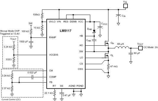 Figure 35. Constant Current Regulator With Hiccup Mode Output OVP
8.4.2 Constant Voltage and Constant Current Regulator
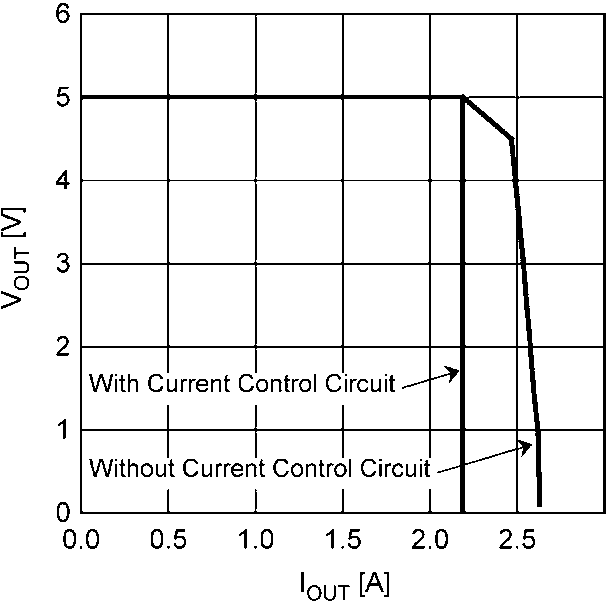
The LM5117 also can be configured as a constant voltage and constant current regulator, known as CV+CC regulator. In this configuration, there is much less variation in the current limiting as compared to peak cycle-by-cycle current limiting of the inductor current. The LMV431 and the PNP transistor create a voltage-to-current amplifier in the current loop. This amplifier circuitry does not affect the normal operation when the output current is less than the current limit set-point. When the output current is greater than the set-point, the PNP transistor sources a current into CRAMP and increases the positive slope of emulated inductor current ramp until the output current is less than or equal to the current limit set-point. See Figure 36 and Figure 37.
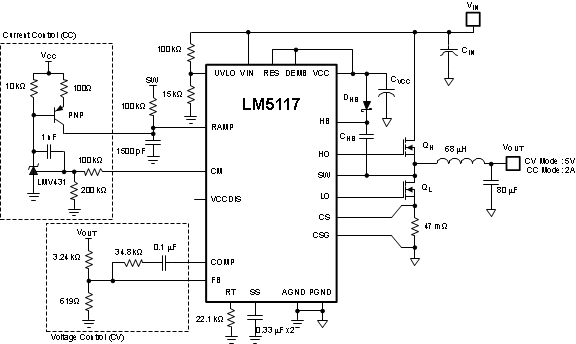 Figure 36. Constant Voltage Regulator with Accurate Current Limit

