SNVSBZ7 October 2021 LM5158 , LM51581
PRODUCTION DATA
- 1 Features
- 2 Applications
- 3 Description
- 4 Revision History
- 5 Description (continued)
- 6 Device Comparison Table
- 7 Pin Configuration and Functions
- 8 Specifications
-
9 Detailed Description
- 9.1 Overview
- 9.2 Functional Block Diagram
- 9.3
Feature Description
- 9.3.1 Line Undervoltage Lockout (EN/UVLO/SYNC Pin)
- 9.3.2 High Voltage VCC Regulator (BIAS, VCC Pin)
- 9.3.3 Soft Start (SS Pin)
- 9.3.4 Switching Frequency (RT Pin)
- 9.3.5 Dual Random Spread Spectrum – DRSS (MODE Pin)
- 9.3.6 Clock Synchronization (EN/UVLO/SYNC Pin)
- 9.3.7 Current Sense and Slope Compensation
- 9.3.8 Current Limit and Minimum On Time
- 9.3.9 Feedback and Error Amplifier (FB, COMP Pin)
- 9.3.10 Power-Good Indicator (PGOOD Pin)
- 9.3.11 Hiccup Mode Overload Protection (MODE Pin)
- 9.3.12 Maximum Duty Cycle Limit and Minimum Input Supply Voltage
- 9.3.13 Internal MOSFET (SW Pin)
- 9.3.14 Overvoltage Protection (OVP)
- 9.3.15 Thermal Shutdown (TSD)
- 9.4 Device Functional Modes
- 10Application and Implementation
- 11Power Supply Recommendations
- 12Layout
- 13Device and Documentation Support
- 14Mechanical, Packaging, and Orderable Information
Package Options
Mechanical Data (Package|Pins)
- RTE|16
Thermal pad, mechanical data (Package|Pins)
- RTE|16
Orderable Information
9.3.7 Current Sense and Slope Compensation
The device senses switch current, which flows into the SW pin and provides a fixed internal slope compensation ramp, which helps prevent subharmonic oscillation at high duty cycle. The internal slope compensation ramp is added to the sensed switch current for the PWM operation. But, no slope compensation ramp is added to the sensed inductor current for the current limit operation to provide an accurate peak current limit over the input supply voltage (see Figure 9-17).
 Figure 9-17 Current Sensing and Slope Compensation
 at PWM Comparator Inputs") Figure 9-18 Current Sensing and Slope Compensation (a) at PWM Comparator Inputs
Figure 9-18 Current Sensing and Slope Compensation (a) at PWM Comparator Inputs at Current Limit Comparator Inputs") Figure 9-19 Current Sensing (b) at Current Limit Comparator Inputs
Figure 9-19 Current Sensing (b) at Current Limit Comparator InputsUse Equation 6 to calculate the value of the peak slope voltage (VSLOPE).
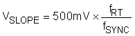
where
- fSYNC is fRT if clock synchronization is not used.
According to peak current mode control theory, the slope of the compensation ramp must be greater than half of the sensed inductor current falling slope to prevent subharmonic oscillation at high duty cycle. Therefore, the minimum amount of slope compensation in boost topology must satisfy the following inequality:
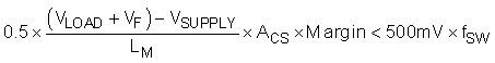
where
- VF is a forward voltage drop of D1, the external diode.
Typically 82% of the sensed inductor current falling slope is known as an optimal amount of the slope compensation. By increasing the margin to 1.6, the amount of slope compensation becomes close to the optimal amount.
If clock synchronization is not used, the fSW frequency equals the fRT frequency. If clock synchronization is used, the fSW frequency equals the fSYNC frequency.