SNVSAF9A August 2016 – November 2017 LM5161-Q1
PRODUCTION DATA.
- 1 Features
- 2 Applications
- 3 Description
- 4 Revision History
- 5 Pin Configuration and Functions
- 6 Specifications
-
7 Detailed Description
- 7.1 Overview
- 7.2 Functional Block Diagram
- 7.3
Feature Description
- 7.3.1 Control Circuit
- 7.3.2 VCC Regulator
- 7.3.3 Regulation Comparator
- 7.3.4 Soft-Start
- 7.3.5 Error Transconductance (GM) Amplifier
- 7.3.6 On-Time Generator
- 7.3.7 Current Limit
- 7.3.8 N-Channel Buck Switch and Driver
- 7.3.9 Synchronous Rectifier
- 7.3.10 Enable / Undervoltage Lockout (EN/UVLO)
- 7.3.11 Thermal Protection
- 7.3.12 Ripple Configuration
- 7.4 Device Functional Modes
-
8 Applications and Implementation
- 8.1 Application Information
- 8.2
Typical Applications
- 8.2.1
LM5161-Q1 Synchronous Buck (15-V to 95-V Input, 12-V Output, 1-A Load)
- 8.2.1.1 Design Requirements
- 8.2.1.2
Detailed Design Procedure
- 8.2.1.2.1 Custom Design With WEBENCH® Tools
- 8.2.1.2.2 Output Resistor Divider Selection
- 8.2.1.2.3 Frequency Selection
- 8.2.1.2.4 Inductor Selection
- 8.2.1.2.5 Output Capacitor Selection
- 8.2.1.2.6 Series Ripple Resistor - RESR (FPWM = 1)
- 8.2.1.2.7 VCC and Bootstrap Capacitor
- 8.2.1.2.8 Input Capacitor Selection
- 8.2.1.2.9 Soft-Start Capacitor Selection
- 8.2.1.2.10 EN/UVLO Resistor Selection
- 8.2.1.3 Application Curves
- 8.2.2 LM5161-Q1 Isolated Fly-Buck (36-V to 72-V Input, 12-V, 12-W Isolated Output)
- 8.2.1
LM5161-Q1 Synchronous Buck (15-V to 95-V Input, 12-V Output, 1-A Load)
- 8.3 Do's and Don'ts
- 9 Power Supply Recommendations
- 10Layout
- 11Device and Documentation Support
- 12Mechanical, Packaging, and Orderable Information
Package Options
Mechanical Data (Package|Pins)
- PWP|14
Thermal pad, mechanical data (Package|Pins)
- PWP|14
Orderable Information
10 Layout
10.1 Layout Guidelines
A proper layout is essential for optimum performance of the circuit. In particular, observe the following layout guidelines:
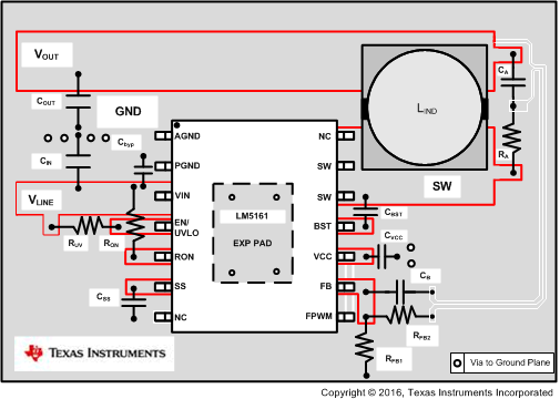
- CIN: The loop consisting of input capacitor (CIN), VIN pin, and PGND pin carries the switching current. Therefore, in the LM5161-Q1, the input capacitor must be placed close to the IC, directly across VIN and PGND pins, and the connections to these two pins should be direct to minimize the loop area. In general it is not possible to place all of input capacitances near the IC. However, a good layout practice includes placing the bulk capacitor as close as possible to the VIN pin (see Figure 41). When using the LM5161-Q1 HTSSOP-14 package, a bypass capacitor (Cbyp) measuring ~0.1 μF must be placed directly across VIN and PGND (pin 3 and 2), as close as possible to the IC while complying with all layout design rules.
- The RON resistor between the VIN and the RON pin and the SS capacitor should be placed as close as possible to their respective pins.
- CVCC and CBST: The VCC and bootstrap (BST) bypass capacitors supply switching currents to the high-side and low-side gate drivers. These two capacitors should also be placed as close to the IC as possible, and the connecting trace lengths and the loop area must be kept at minimum (see Figure 41).
- The feedback trace carries the output voltage information and a small ripple component that is necessary for proper operation of the LM5161-Q1. Therefore, care must be taken while routing the feedback trace to avoid coupling any noise into this pin. In particular, the feedback trace must be short and not run close to magnetic components, or parallel to any other switching trace.
- In FPWM=1 mode, if a ripple injection circuit is being used for ripple generation at the FB pin, it is considered a good layout practice to lay out the feedback ripple injection DC trace and the VOUT trace differentially. This scheme helps in reducing the scope for any noise injection at the FB pin.
- SW trace: The SW node switches rapidly between VIN and GND every cycle and is therefore a source of noise. The SW node area must be kept at minimum. In particular, the SW node should not be inadvertently connected to a copper plane or pour.
10.2 Layout Example
 Figure 41. Typical Buck Layout Example