SNVSBB3A October 2019 – April 2024 LM5163
PRODUCTION DATA
- 1
- 1 Features
- 2 Applications
- 3 Description
- 4 Pin Configuration and Functions
- 5 Specifications
-
6 Detailed Description
- 6.1 Overview
- 6.2 Functional Block Diagram
- 6.3
Feature Description
- 6.3.1 Control Architecture
- 6.3.2 Internal VCC Regulator and Bootstrap Capacitor
- 6.3.3 Regulation Comparator
- 6.3.4 Internal Soft Start
- 6.3.5 On-Time Generator
- 6.3.6 Current Limit
- 6.3.7 N-Channel Buck Switch and Driver
- 6.3.8 Synchronous Rectifier
- 6.3.9 Enable/Undervoltage Lockout (EN/UVLO)
- 6.3.10 Power Good (PGOOD)
- 6.3.11 Thermal Protection
- 6.4 Device Functional Modes
- 7 Application and Implementation
- 8 Device and Documentation Support
- 9 Revision History
- 10Mechanical, Packaging, and Orderable Information
Package Options
Mechanical Data (Package|Pins)
- DDA|8
Thermal pad, mechanical data (Package|Pins)
- DDA|8
Orderable Information
7.2.2.5 Input Capacitor (CIN)
An input capacitor is necessary to limit the input ripple voltage while providing AC current to the buck power stage at every switching cycle. To minimize the parasitic inductance in the switching loop, position the input capacitors as close as possible to the VIN and GND pins of the LM5163. The input capacitors conduct a square-wave current of peak-to-peak amplitude equal to the output current. It follows that the resultant capacitive component of AC ripple voltage is a triangular waveform.
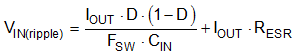
Along with the ESR-related ripple component, use Equation 22 to calculate the peak-to-peak ripple voltage amplitude.
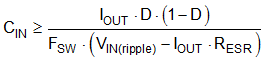
Use Equation 23 to calculate the input capacitance required for a load current, based on an input voltage ripple specification (ΔVIN).
The recommended high-frequency input capacitance is 2.2 µF or higher. Ensure the input capacitor is a high-quality X7S or X7R ceramic capacitor with sufficient voltage rating for CIN. Based on the voltage coefficient of ceramic capacitors, choose a voltage rating of twice the maximum input voltage. Additionally, some bulk capacitance is required if the LM5163 is not located within approximately 5 cm from the input voltage source. This capacitor provides parallel damping to the resonance associated with parasitic inductance of the supply lines and high-Q ceramics. See the Section 7.3 section for more detail.