SNVSB46B September 2018 – August 2021 LM5176-Q1
PRODUCTION DATA
- 1 Features
- 2 Applications
- 3 Description
- 4 Revision History
- 5 Pin Configuration and Functions
- 6 Specifications
-
7 Detailed Description
- 7.1 Overview
- 7.2 Functional Block Diagram
- 7.3
Feature Description
- 7.3.1 Fixed Frequency Valley/Peak Current Mode Control with Slope Compensation
- 7.3.2 VCC Regulator and Optional BIAS Input
- 7.3.3 Enable/UVLO
- 7.3.4 Soft-Start
- 7.3.5 Overcurrent Protection
- 7.3.6 Average Input/Output Current Limiting
- 7.3.7 Operation Above 40-V Input
- 7.3.8 CCM Operation
- 7.3.9 Frequency and Synchronization (RT/SYNC)
- 7.3.10 Frequency Dithering
- 7.3.11 Output Overvoltage Protection (OVP)
- 7.3.12 Power Good (PGOOD)
- 7.3.13 Gm Error Amplifier
- 7.3.14 Integrated Gate Drivers
- 7.3.15 Thermal Shutdown
- 7.4 Device Functional Modes
-
8 Application and Implementation
- 8.1 Application Information
- 8.2
Typical Application
- 8.2.1 Design Requirements
- 8.2.2
Detailed Design Procedure
- 8.2.2.1 Custom Design with WEBENCH Tools
- 8.2.2.2 Frequency
- 8.2.2.3 VOUT
- 8.2.2.4 Inductor Selection
- 8.2.2.5 Output Capacitor
- 8.2.2.6 Input Capacitor
- 8.2.2.7 Sense Resistor (RSENSE)
- 8.2.2.8 Slope Compensation
- 8.2.2.9 UVLO
- 8.2.2.10 Soft-Start Capacitor
- 8.2.2.11 Dither Capacitor
- 8.2.2.12 MOSFETs QH1 and QL1
- 8.2.2.13 MOSFETs QH2 and QL2
- 8.2.2.14 Frequency Compensation
- 8.2.3 Application Curves
- 9 Power Supply Recommendations
- 10Layout
- 11Device and Documentation Support
- 12Mechanical, Packaging, and Orderable Information
Package Options
Mechanical Data (Package|Pins)
- PWP|28
Thermal pad, mechanical data (Package|Pins)
- PWP|28
Orderable Information
8.2.2.7 Sense Resistor (RSENSE)
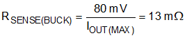
The current sense resistor between the CS and CSG pins should be selected to ensure that current limit is set high enough for both buck and boost modes of operation. For the buck operation, the current limit resistor is given by:
For the boost mode of operation, the current limit resistor is given by:
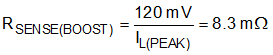
The closest standard value of RSENSE = 8 mΩ is selected based on the boost mode operation.
The maximum power dissipation in RSENSE happens at VIN(MIN):
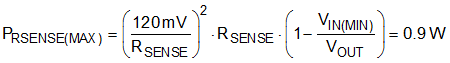
Therefore, a sense resistor with 2-W power rating will be sufficient for this application.
For some application circuits, it can be required to add a filter network to attenuate noise in the CS and CSG sense lines. See Figure 8-1 for typical values. The filter resistance should not exceed 100 Ω.