SNIS152E May 2009 – July 2015 LM57
PRODUCTION DATA.
- 1 Features
- 2 Applications
- 3 Description
- 4 Revision History
- 5 Device Comparison Table
- 6 Pin Configuration and Functions
-
7 Specifications
- 7.1 Absolute Maximum Ratings
- 7.2 ESD Ratings
- 7.3 Recommended Operating Conditions
- 7.4 Thermal Information
- 7.5 Electrical Characteristics - Accuracy Characteristics - Trip Point Accuracy
- 7.6 Electrical Characteristics - Accuracy Characteristics - VTEMP Analog Temperature Sensor Output Accuracy
- 7.7 Electrical Characteristics
- 7.8 Switching Characteristics
- 7.9 Typical Characteristics
-
8 Detailed Description
- 8.1 Overview
- 8.2 Functional Block Diagram
- 8.3 Feature Description
- 8.4 Device Functional Modes
- 9 Application and Implementation
- 10Power Supply Recommendations
- 11Layout
- 12Device and Documentation Support
- 13Mechanical, Packaging, and Orderable Information
Package Options
Mechanical Data (Package|Pins)
Thermal pad, mechanical data (Package|Pins)
Orderable Information
7 Specifications
7.1 Absolute Maximum Ratings
over operating free-air temperature range (unless otherwise noted) (1)(2)| MIN | MAX | UNIT | ||
|---|---|---|---|---|
| Supply voltage | −0.3 | 6 | V | |
| Voltage at TOVER | −0.3 | 6 | V | |
| Voltage at TOVER , VTEMP, TRIP-TEST, SENSE1, and SENSE2 | −0.3 | (VDD + 0.3 V) | V | |
| Current at any pin | 5 | mA | ||
| Storage temperature | −65 | 150 | °C | |
(1) Stresses beyond those listed under Absolute Maximum Ratings may cause permanent damage to the device. These are stress ratings only, which do not imply functional operation of the device at these or any other conditions beyond those indicated under Recommended Operating Conditions. Exposure to absolute-maximum-rated conditions for extended periods may affect device reliability.
(2) Soldering process must comply with Reflow Temperature Profile specifications. Refer to www.ti.com/packaging.
7.2 ESD Ratings
| VALUE | UNIT | |||
|---|---|---|---|---|
| LM57BISD and LM57CISD in WSON package | ||||
| V(ESD) | Electrostatic discharge (1) | Human body model (HBM) | ±5500 | V |
| Charged-device model (CDM) | ±1250 | |||
| Machine Model (MM) | ±450 | |||
| LM57FPW and LM57TPW in TSSOP package | ||||
| V(ESD) | Electrostatic discharge | Human body model (HBM), per ANSI/ESDA/JEDEC JS-001 (2) | ±2000 | V |
| Charged-device model (CDM), per JEDEC specification JESD22-C101 (3) | ±750 | |||
(1) The Human Body Model (HBM) is a 100-pF capacitor charged to the specified voltage then discharged through a 1.5-kΩ resistor into each pin. The Machine Model (MM) is a 200 pF capacitor charged to the specified voltage then discharged directly into each pin. The Charged Device Model (CDM) is a specified circuit characterizing an ESD event that occurs when a device acquires charge through some triboelectric (frictional) or electrostatic induction processes and then abruptly touches a grounded object or surface.
(2) JEDEC document JEP155 states that 500-V HBM allows safe manufacturing with a standard ESD control process.
(3) JEDEC document JEP157 states that 250-V CDM allows safe manufacturing with a standard ESD control process.
7.3 Recommended Operating Conditions
| MIN | NOM | MAX | UNIT | ||
|---|---|---|---|---|---|
| Supply voltage | 2.4 | 5.5 | V | ||
| Free air temperature range (TMIN ≤ TA ≤ TMAX) | −50 | 150 | °C | ||
7.4 Thermal Information
| THERMAL METRIC (1) | LM57 | UNIT | ||
|---|---|---|---|---|
| NGR (WSON/SD) | PW (TSSOP) | |||
| 8 PINS | 8 PINS | |||
| RθJA | Junction-to-ambient thermal resistance | 71.3 | 183 | °C/W |
| RθJC(top) | Junction-to-case (top) thermal resistance | 82.8 | 66 | °C/W |
| RθJB | Junction-to-board thermal resistance | 43.4 | 111 | °C/W |
| ψJT | Junction-to-top characterization parameter | 2.2 | 8 | °C/W |
| ψJB | Junction-to-board characterization parameter | 43.7 | 110 | °C/W |
| RθJC(bot) | Junction-to-case (bottom) thermal resistance | 11.9 | — | °C/W |
(1) For more information about traditional and new thermal metrics, see the Semiconductor and IC Package Thermal Metrics application report, SPRA953.
7.5 Electrical Characteristics - Accuracy Characteristics – Trip Point Accuracy
| PARAMETER | TEST CONDITIONS | LM57B | LM57C, LM57F or LM57T | UNIT | ||||||
|---|---|---|---|---|---|---|---|---|---|---|
| MIN | TYP | MAX | MIN | TYP | MAX | |||||
| Trip Point Accuracy (Includes 1% set-resistor tolerance) (1) |
J2 | TA = −41°C to 52°C | VDD = 2.4 V to 5.5 V | ±1.5 | ±2.3 | °C | ||||
| J3 | TA = 52°C to 97°C | VDD = 2.4 V to 5.5 V | ±1.5 | ±2.3 | °C | |||||
| J4 | TA = 97°C to 119°C | VDD = 2.4 V to 5.5 V | ±1.5 | ±2.3 | °C | |||||
| J5 | TA = 119°C to free air temperature max | VDD = 2.4 V to 5.5 V | ±1.5 | ±2.3 | °C | |||||
(1) Accuracy is defined as the error between the measured and reference output voltages, tabulated in the Conversion Table at the specified conditions of supply gain setting, voltage, and temperature (expressed in °C). Accuracy limits include line regulation within the specified conditions. Accuracy limits do not include load regulation; they assume no DC load.
7.6 Electrical Characteristics - Accuracy Characteristics – VTEMP Analog Temperature Sensor Output Accuracy
These limits do not include DC load regulation. These stated accuracy limits are with reference to the values in Table 1.| PARAMETER | TEST CONDITIONS | LM57B | LM57C, LM57F or LM57T | UNIT | ||||||
|---|---|---|---|---|---|---|---|---|---|---|
| MIN | TYP | MAX | MIN | TYP | MAX | |||||
| VTEMP Accuracy (These stated accuracy limits are with reference to the values in Table 1, LM57 VTEMP Temperature-to-Voltage.) (1) |
J2 | TA = −50°C to free air temperature max | VDD = 2.4 V to 5.5 V | ±0.95 | ±1.3 | °C | ||||
| J3 | TA = −50°C to free air temperature max | VDD = 2.4 V to 5.5 V | ±0.8 | ±1.3 | °C | |||||
| J4 | TA = 20°C to 50°C | VDD = 2.4 V to 5.5 V | ±0.7 | ±1.3 | °C | |||||
| TA = 0°C to free air temperature max | VDD = 2.7 V to 5.5 V | ±0.7 | ±1.3 | |||||||
| TA = −50°C to 0°C | VDD = 3.1 V to 5.5 V | ±0.8 | ±1.3 | |||||||
| J5 | TA = 60°C to free air temperature max | VDD = 2.4 V to 5.5 V | ±0.7 | ±1.3 | °C | |||||
| TA = 20°C to 50°C | VDD = 2.9 V to 5.5 V | ±0.7 | ±1.3 | |||||||
| TA = 0°C to free air temperature max | VDD = 3.2 V to 5.5 V | ±0.7 | ±1.3 | |||||||
| TA = −50°C to 0°C | VDD = 4 V to 5.5 V | ±0.8 | ±1.3 | |||||||
(1) Accuracy is defined as the error between the measured and reference output voltages, tabulated in the Conversion Table at the specified conditions of supply gain setting, voltage, and temperature (expressed in °C). Accuracy limits include line regulation within the specified conditions. Accuracy limits do not include load regulation; they assume no DC load.
7.7 Electrical Characteristics
Unless otherwise noted, these specifications apply for VDD = 2.4 to 5.5 V. Limits apply over free air temperature range.| PARAMETER | TEST CONDITIONS | MIN (2) | TYP (1) | MAX (2) | UNIT | |
|---|---|---|---|---|---|---|
| TEMPERATURE SENSOR | ||||||
| VTEMP sensor gain | J2: −50°C to 52°C | −5.166 | mV/°C | |||
| J3: 52°C to 97°C | −7.752 | |||||
| J4: 97°C to 119°C | −10.339 | |||||
| J5: 119°C to 150°C | −12.924 | |||||
| Line regulation DC: supply-to-VTEMP(3) | VDD = 2.4 V to 5.5 V Temp = 90°C |
0.18 | mV | |||
| 58 | μV/V | |||||
| −84 | dB | |||||
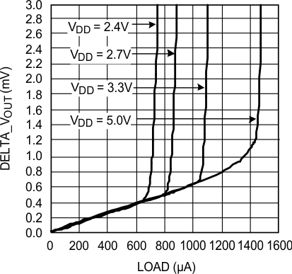
| Load regulation: VTEMP output (6) | Source ≤ 240 µA, (VDD – VTEMP) ≥ 200 mV; TA = −50°C to 150°C | −1 | mV | |||
| Sink ≤ 300 µA, VTEMP ≥ 360 mV; TA = −50°C to 150°C | 1 | |||||
| Source or sink = 100 µA; TA = −50°C to 150°C | 1 | Ω | ||||
| Maximum Load capacitance: VTEMP output | No output series resistor required; (See VTEMP Capacitive Loads) | 1100 | pF | |||
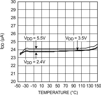
| IS | Supply current: quiescent (4) | 24 | 28 | µA | ||
| TRIP-TEST INPUT | ||||||
| VIH | Logic 1 threshold voltage | VDD – 0.5 | V | |||
| VIL | Logic 0 threshold voltage | 0.5 | V | |||
| IIH | Logic 1 input current | 1.4 | 3 | µA | ||
| IIL | Logic 0 input leakage current (5) | TA = −50°C to 150°C | 0.001 | 1 | µA | |
| TOVER (PUSH-PULL, ACTIVE-HIGH) OUTPUT | ||||||
| VOH | Logic 1 push-pull output voltage | Source ≤ 600 µA | VDD – 0.2 | V | ||
| Source ≤ 1.2 mA | VDD – 0.45 | |||||
| VOL | Logic 0 output voltage | Sink ≤ 600 µA | 0.2 | V | ||
| Sink ≤ 1.2 mA | 0.45 | |||||
| TOVER (OPEN-DRAIN, ACTIVE-LOW) OUTPUT | ||||||
| VOL | Logic 0 output voltage | Sink ≤ 600 µA | 0.2 | V | ||
| Sink ≤1.2 mA | 0.45 | |||||
| IOH | Logic 1 output leakage current (5) | Temperature = 30°C; | 0.001 | 1 | µA | |
| HYSTERESIS | ||||||
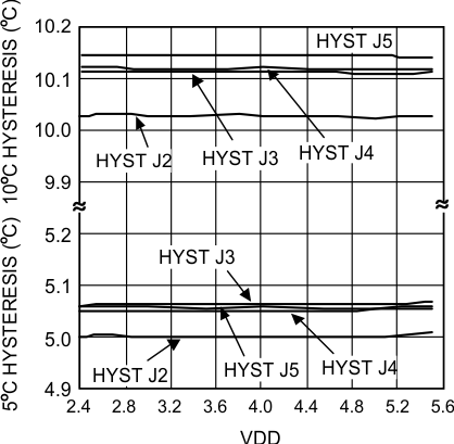
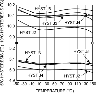
| THYST | Hysteresis temperature | 5°C hysteresis option (for all LM57F or LM57-5) | 4.7 | 5 | 5.4 | °C |
| 10°C hysteresis option (for all LM57T or LM57-10) | 9.6 | 10 | 10.6 | °C | ||
(1) Typicals are at TJ = TA = 25°C and represent most likely parametric norm.
(2) Limits are specified to TI's average outgoing quality level (AOQL).
(3) Line regulation (DC) is calculated by subtracting the output voltage at the highest supply voltage from the output voltage at the lowest supply voltage. The typical DC line regulation specification does not include the output voltage shift discussed in VTEMP Voltage Shift.
(4) Supply current refers to the quiescent current of the LM57 only and does not include any load current
(5) This current is leakage current only and is therefore highest at high temperatures. Prototype test indicate that the leakage is well below 1 μA over the full temperature range. This 1 μA specification reflects the limitations of measuring leakage at room temperature. For this reason only, the leakage current is not specified at a lower value.
(6) Source currents are flowing out of the LM57. Sink currents are flowing into the LM57. Load Regulation is calculated by measuring VTEMP at 0 μA and subtracting the value with the conditions specified.
7.8 Switching Characteristics
Unless otherwise noted, these specifications apply for VDD = 2.4 to 5.5 V over the free air temperature range.| PARAMETER | TEST CONDITIONS | MIN | TYP | MAX | UNIT | ||
|---|---|---|---|---|---|---|---|
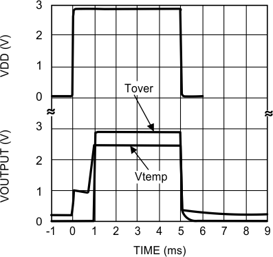
| tEN | Maximum time from power on to digital output enabled | 1.5 | 2.9 | ms | |||
| tVTEMP | Maximum time from power on to analog temperature (VTEMP) valid | 1.5 | 2.9 | ms | |||
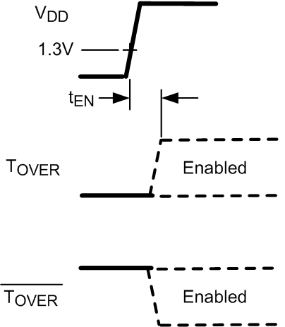 Figure 1. Definition of tEN
 Figure 2. Definition of tVTEMP
7.9 Typical Characteristics
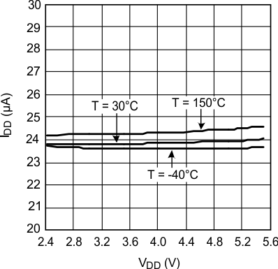
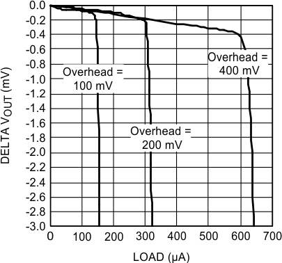
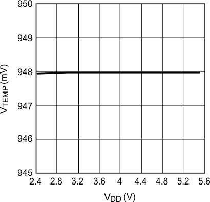
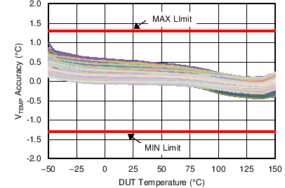
| Conditions: J2, VDD=5V |
