SNOS751E April 2000 – September 2014 LM6132 , LM6134
PRODUCTION DATA.
- 1Features
- 2Applications
- 3Description
- 4Revision History
- 5Pin Configuration and Functions
-
6Specifications
- 6.1 Absolute Maximum Ratings
- 6.2 Handling Ratings
- 6.3 Recommended Operating Conditions
- 6.4 Thermal Information, 8-Pin
- 6.5 Thermal Information, 14-Pin
- 6.6 5.0V DC Electrical Characteristics
- 6.7 5.0V AC Electrical Characteristics
- 6.8 2.7V DC Electrical Characteristics
- 6.9 2.7V AC Electrical Characteristics
- 6.10 24V DC Electrical Characteristics
- 6.11 24V AC Electrical Characteristics
- 6.12 Typical Performance Characteristics
- 7Application and Implementation
- 8Device and Documentation Support
- 9Mechanical, Packaging, and Orderable Information
Package Options
Mechanical Data (Package|Pins)
Thermal pad, mechanical data (Package|Pins)
Orderable Information
6 Specifications
6.1 Absolute Maximum Ratings(1)(6)
over operating free-air temperature range (unless otherwise noted)| MIN | MAX | UNIT | |
|---|---|---|---|
| Differential Input Voltage | ±15 | V | |
| Voltage at Input/Output Pin | (V+)+0.3 (V−)−0.3 |
V | |
| Supply Voltage (V+–V−) | 35 | V | |
| Current at Input Pin | ±10 | mA | |
| Current at Output Pin(2) | ±25 | mA | |
| Current at Power Supply Pin | 50 | mA | |
| Lead Temp. (soldering, 10 sec.) | 260 | °C | |
| Junction Temperature(3) | 150 | °C |
6.2 Handling Ratings
| MIN | MAX | UNIT | |||
|---|---|---|---|---|---|
| Tstg | Storage temperature range | −65 | +150 | °C | |
| V(ESD) | Electrostatic discharge | Human body model (HBM), per ANSI/ESDA/JEDEC JS-001, all pins(1) | 2500 | V | |
(1) Human Body Model, 1.5 kΩ in series with 100 pF .JEDEC document JEP155 states that 2500-V HBM allows safe manufacturing with a standard ESD control process.
6.3 Recommended Operating Conditions(1)
over operating free-air temperature range (unless otherwise noted)| MIN | MAX | UNIT | ||
|---|---|---|---|---|
| Supply Voltage | 1.8 ≤ V+ ≤ 24 | V | ||
| Operating Temperature Range: LM6132, LM6134 | −40 | +85 | °C | |
6.4 Thermal Information, 8-Pin
| THERMAL METRIC(1) | D (SOIC) | P (PDIP) | UNIT | |
|---|---|---|---|---|
| 8 PINS | 8 PINS | |||
| RθJA | Junction-to-ambient thermal resistance | 193 | 115 | °C/W |
(1) For more information about traditional and new thermal metrics, see the IC Package Thermal Metrics application report, SPRA953.
6.5 Thermal Information, 14-Pin
| THERMAL METRIC(1) | D (SOIC) | NFF (PDIP) | UNIT | |
|---|---|---|---|---|
| 14 PINS | 14 PINS | |||
| RθJA | Junction-to-ambient thermal resistance | 126 | 81 | °C/W |
(1) For more information about traditional and new thermal metrics, see the IC Package Thermal Metrics application report, SPRA953.
6.6 5.0V DC Electrical Characteristics
Unless otherwise specified, all limits guaranteed for V+ = 5.0V, V− = 0V, VCM = VO = V+/2 and RL > 1 MΩ to V+/2. Boldface limits apply at the temperature extremes| PARAMETER | TEST CONDITIONS | TYP(4) | LM6134AI LM6132AI LIMIT(5) |
LM6134BI LM6132BI LIMIT(5) |
UNIT | |
|---|---|---|---|---|---|---|
| VOS | Input Offset Voltage | 0.25 | 2 4 |
6 8 |
mV max |
|
| TCVOS | Input Offset Voltage Average Drift | 5 | μV/C | |||
| IB | Input Bias Current | 0V ≤ VCM ≤ 5V | 110 | 140 300 |
180 350 |
nA max |
| IOS | Input Offset Current | 3.4 | 30 50 |
30 50 |
nA max |
|
| RIN | Input Resistance, CM | 104 | MΩ | |||
| CMRR | Common Mode Rejection Ratio | 0V ≤ VCM ≤ 4V | 100 | 75 70 |
75 70 |
dB min |
| 0V ≤ VCM ≤ 5V | 80 | 60 55 |
60 55 |
|||
| PSRR | Power Supply Rejection Ratio | ±2.5V ≤ V+ ≤ ±12V | 82 | 78 75 |
78 75 |
dB min |
| VCM | Input Common-Mode Voltage Range | −0.25 5.25 |
0
5.0 |
0
5.0 |
V | |
| AV | Large Signal Voltage Gain | RL = 10k | 100 | 25 8 |
15 6 |
V/mV min |
| VO | Output Swing | 100k Load | 4.992 | 4.98 4.93 |
4.98 4.93 |
V min |
| 0.007 | 0.017 0.019 |
0.017 0.019 |
V max |
|||
| 10k Load | 4.952 | 4.94 4.85 |
4.94 4.85 |
V min |
||
| 0.032 | 0.07 0.09 |
0.07 0.09 |
V max |
|||
| 5k Load | 4.923 | 4.90 4.85 |
4.90 4.85 |
V min |
||
| 0.051 | 0.095 0.12 |
0.095 0.12 |
V max |
|||
| ISC | Output Short Circuit Current LM6132 |
Sourcing | 4 | 2 2 |
2 1 |
mA min |
| Sinking | 3.5 | 1.8 1.8 |
1.8 1 |
mA min |
||
| ISC | Output Short Circuit Current LM6134 |
Sourcing | 3 | 2 1.6 |
2 1 |
mA min |
| Sinking | 3.5 | 1.8 1.3 |
1.8 1 |
mA min |
||
| IS | Supply Current | Per Amplifier | 360 | 400 450 |
400 450 |
μA max |
6.7 5.0V AC Electrical Characteristics
Unless otherwise specified, all limits guaranteed for V+ = 5.0V, V− = 0V, VCM = VO = V+/2 and RL > 1 MΩ to V+/2. Boldface limits apply at the temperature extremes| PARAMETER | TEST CONDITIONS | TYP(4) | LM6134AI LM6132AI LIMIT(5) |
LM6134BI LM6132BI LIMIT(5) |
UNIT | |
|---|---|---|---|---|---|---|
| SR | Slew Rate | ±4V @ VS = ±6V RS < 1 kΩ |
14 | 8 7 |
8 7 |
V/μs min |
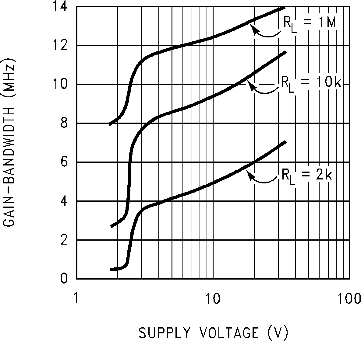
| GBW | Gain-Bandwidth Product | f = 20 kHz | 10 | 7.4 7 |
7.4 7 |
MHz min |
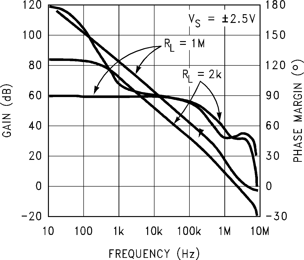
| θm | Phase Margin | RL = 10k | 33 | deg | ||
| Gm | Gain Margin | RL = 10k | 10 | dB | ||
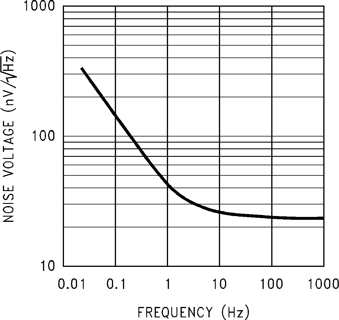
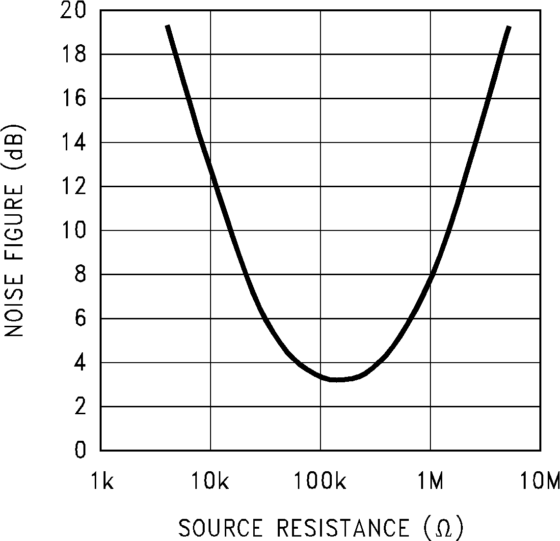
| en | Input Referred Voltage Noise | f = 1 kHz | 27 | nV/√Hz | ||
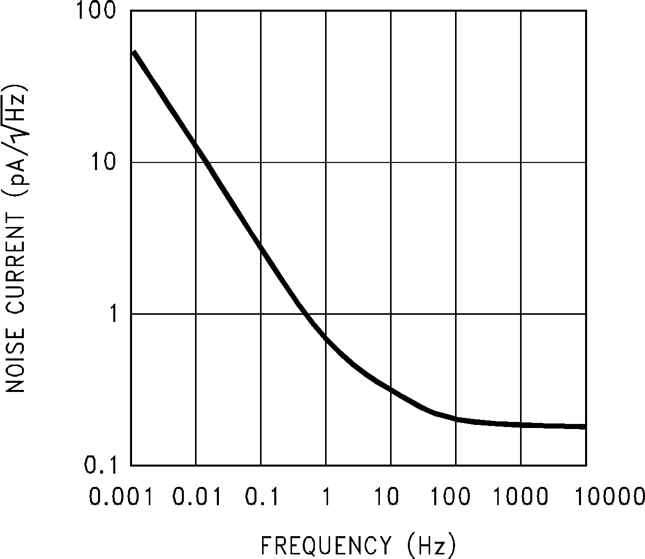
| in | Input Referred Current Noise | f = 1 kHz | 0.18 | pA/√Hz |
6.8 2.7V DC Electrical Characteristics
Unless otherwise specified, all limits guaranteed for V+ = 2.7V, V− = 0V, VCM = VO = V+/2 and RL > 1 MΩ to V+/2. Boldface limits apply at the temperature extreme| PARAMETER | TEST CONDITIONS | TYP(4) | LM6134AI LM6132AI LIMIT(5) |
LM6134BI LM6132BI LIMIT(5) |
UNIT | |
|---|---|---|---|---|---|---|
| VOS | Input Offset Voltage | 0.12 | 2 8 |
6 12 |
mV max |
|
| IB | Input Bias Current | 0V ≤ VCM ≤ 2.7V | 90 | nA | ||
| IOS | Input Offset Current | 2.8 | nA | |||
| RIN | Input Resistance | 134 | MΩ | |||
| CMRR | Common Mode Rejection Ratio | 0V ≤ VCM ≤ 2.7V | 82 | dB | ||
| PSRR | Power Supply Rejection Ratio | ±1.35V ≤ V+ ≤ ±12V | 80 | dB | ||
| VCM | Input Common-Mode Voltage Range | 2.7 0 |
2.7 0 |
V | ||
| AV | Large Signal Voltage Gain | RL = 10k | 100 | V/mV | ||
| VO | Output Swing | RL = 100k | 0.03 | 0.08 0.112 |
0.08 0.112 |
V max |
| 2.66 | 2.65 2.25 |
2.65 2.25 |
V min |
|||
| IS | Supply Current | Per Amplifier | 330 | μA |
6.9 2.7V AC Electrical Characteristics
Unless otherwise specified, all limits guaranteed for V+ = 2.7V, V− = 0V, VCM = VO = V+/2 and RL > 1 MΩ to V+/2.| PARAMETER | TEST CONDITIONS | TYP (4) |
LM6134AI LM6132AI LIMIT (5) |
LM6134BI LM6132BI LIMIT (5) |
UNIT | |
|---|---|---|---|---|---|---|
| GBW | Gain-Bandwidth Product | RL = 10k, f = 20 kHz | 7 | MHz | ||
| θm | Phase Margin | RL = 10k | 23 | deg | ||
| Gm | Gain Margin | 12 | dB |
6.10 24V DC Electrical Characteristics
Unless otherwise specified, all limits guaranteed for V+ = 24V, V− = 0V, VCM = VO = V+/2 and RL > 1 MΩ to V+/2. Boldface limits apply at the temperature extreme| PARAMETER | TEST CONDITIONS | TYP(4) | LM6134AI LM6132AI LIMIT(5) |
LM6134BI LM6132BI LIMIT(5) |
UNIT | |
|---|---|---|---|---|---|---|
| VOS | Input Offset Voltage | 1.7 | 3 5 |
7 9 |
mV max |
|
| IB | Input Bias Current | 0V ≤ VCM ≤ 24V | 125 | nA | ||
| IOS | Input Offset Current | 4.8 | nA | |||
| RIN | Input Resistance | 210 | MΩ | |||
| CMRR | Common Mode Rejection Ratio | 0V ≤ VCM ≤ 24V | 80 | dB | ||
| PSRR | Power Supply Rejection Ratio | 2.7V ≤ V+ ≤ 24V | 82 | dB | ||
| VCM | Input Common-Mode Voltage Range | −0.25 24.25 |
0 24 |
0 24 |
V min V max |
|
| AV | Large Signal Voltage Gain | RL = 10k | 102 | V/mV | ||
| VO | Output Swing | RL = 10k | 0.075 23.86 |
0.15 23.8 |
0.15 23.8 |
V max |
| V min |
||||||
| IS | Supply Current | Per Amplifier | 390 | 450 490 |
450 490 |
μA max |
6.11 24V AC Electrical Characteristics
Unless otherwise specified, all limits guaranteed for V+ = 24V, V− = 0V, VCM = VO = V+/2 and RL > 1 MΩ to V+/2.| PARAMETER | TEST CONDITIONS | TYP(4) | LM6134AI LM6132AI LIMIT(5) |
LM6134BI LM6132BI LIMIT(5) |
UNIT | |
|---|---|---|---|---|---|---|
| GBW | Gain-Bandwidth Product | RL = 10k, f = 20 kHz | 11 | MHz | ||
| θm | Phase Margin | RL = 10k | 23 | deg | ||
| Gm | Gain Margin | RL = 10k | 12 | dB | ||
| THD + N | Total Harmonic Distortion and Noise | AV = +1, VO = 20VP-P
f = 10 kHz |
0.0015% |
(1) Absolute Maximum Ratings indicate limits beyond which damage to the device may occur. Operating Ratings indicate conditions for which the device is intended to be functional, but specific performance is not guaranteed. For guaranteed specifications and the test conditions, see the Electrical characteristics.
(2) Applies to both single-supply and split-supply operation. Continuous short circuit operation at elevated ambient temperature can result in exceeding the maximum allowed junction temperature of 150°C.
(3) The maximum power dissipation is a function of TJ(MAX), RθJA, and TA. The maximum allowable power dissipation at any ambient temperature is PD = (TJ(MAX) − TA)/RθJA. All numbers apply for packages soldered directly into a PC board.
(4) Typical Values represent the most likely parametric normal.
(5) All limits are guaranteed by testing or statistical analysis.
(6) If Military/Aerospace specified devices are required, please contact the Texas Instruments Sales Office/Distributors for availability and specifications.
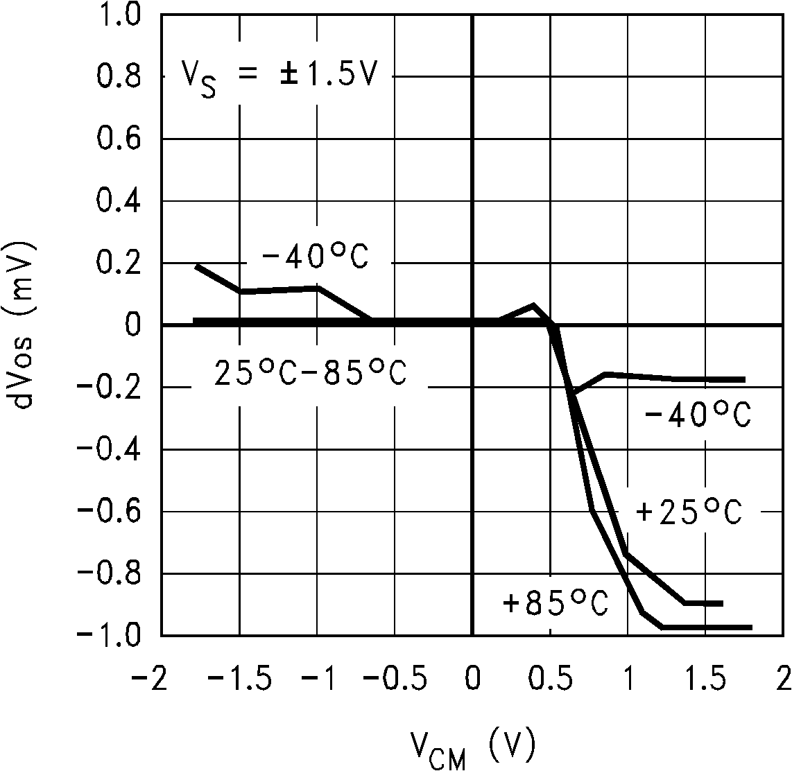
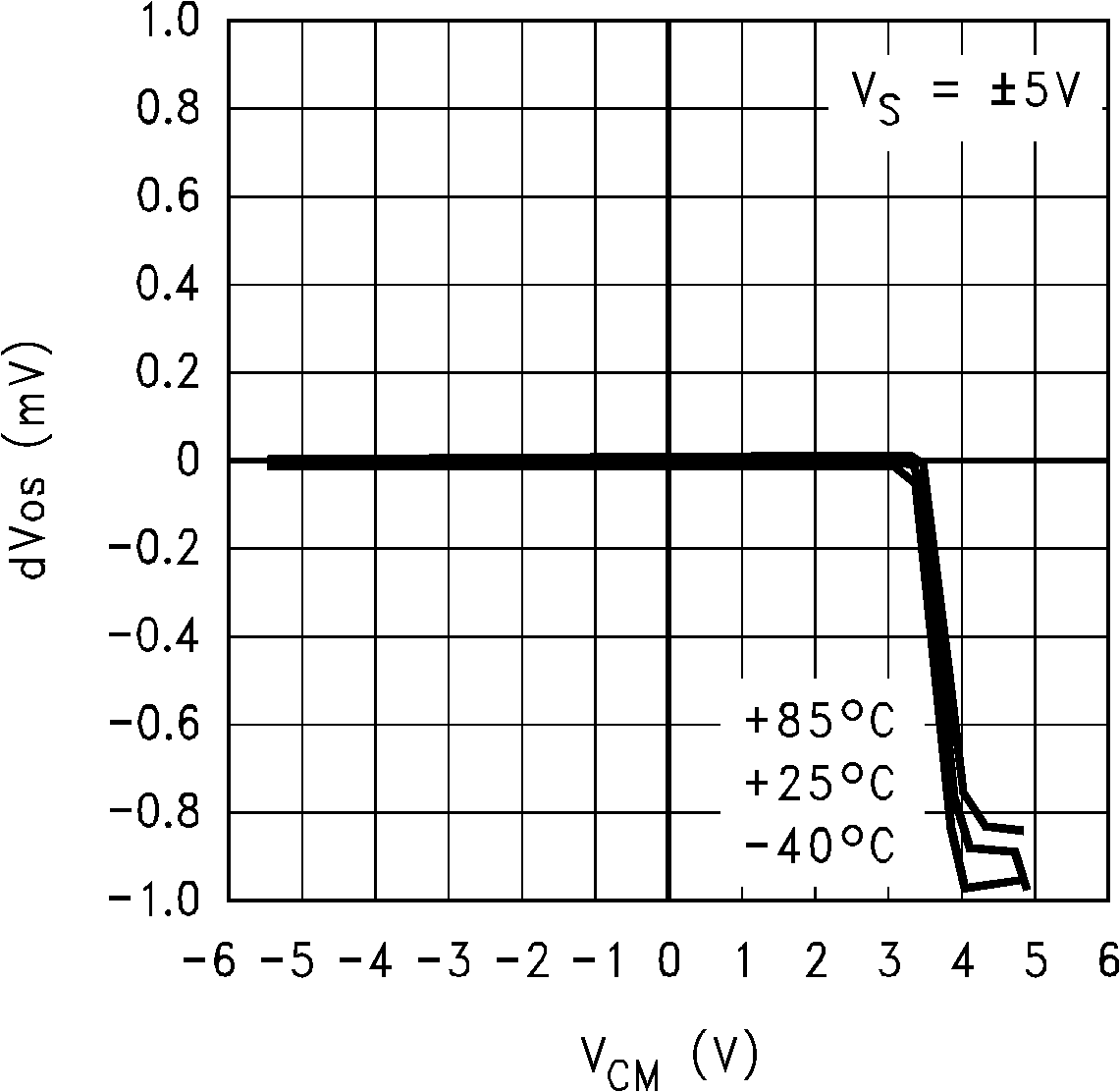
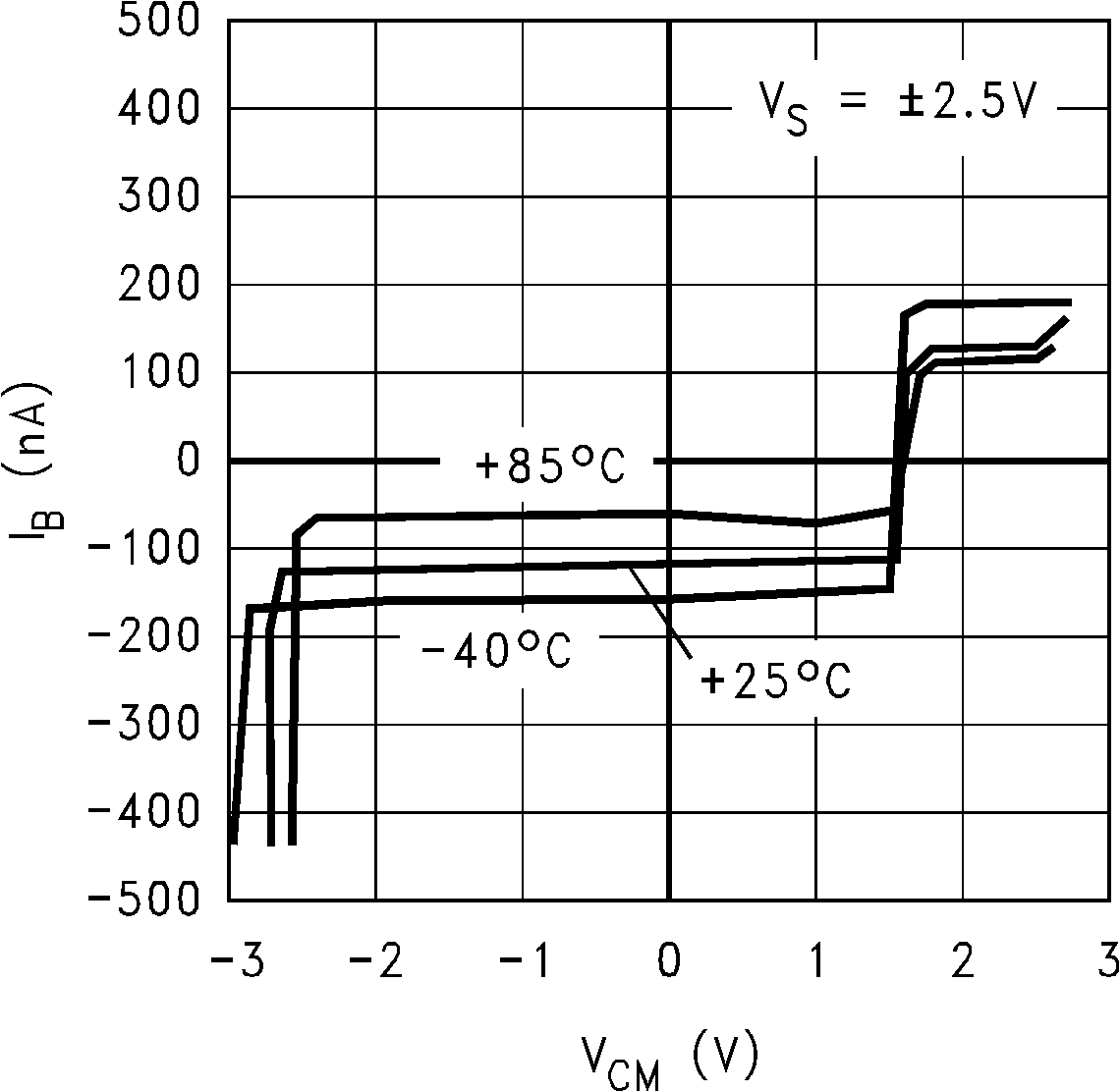
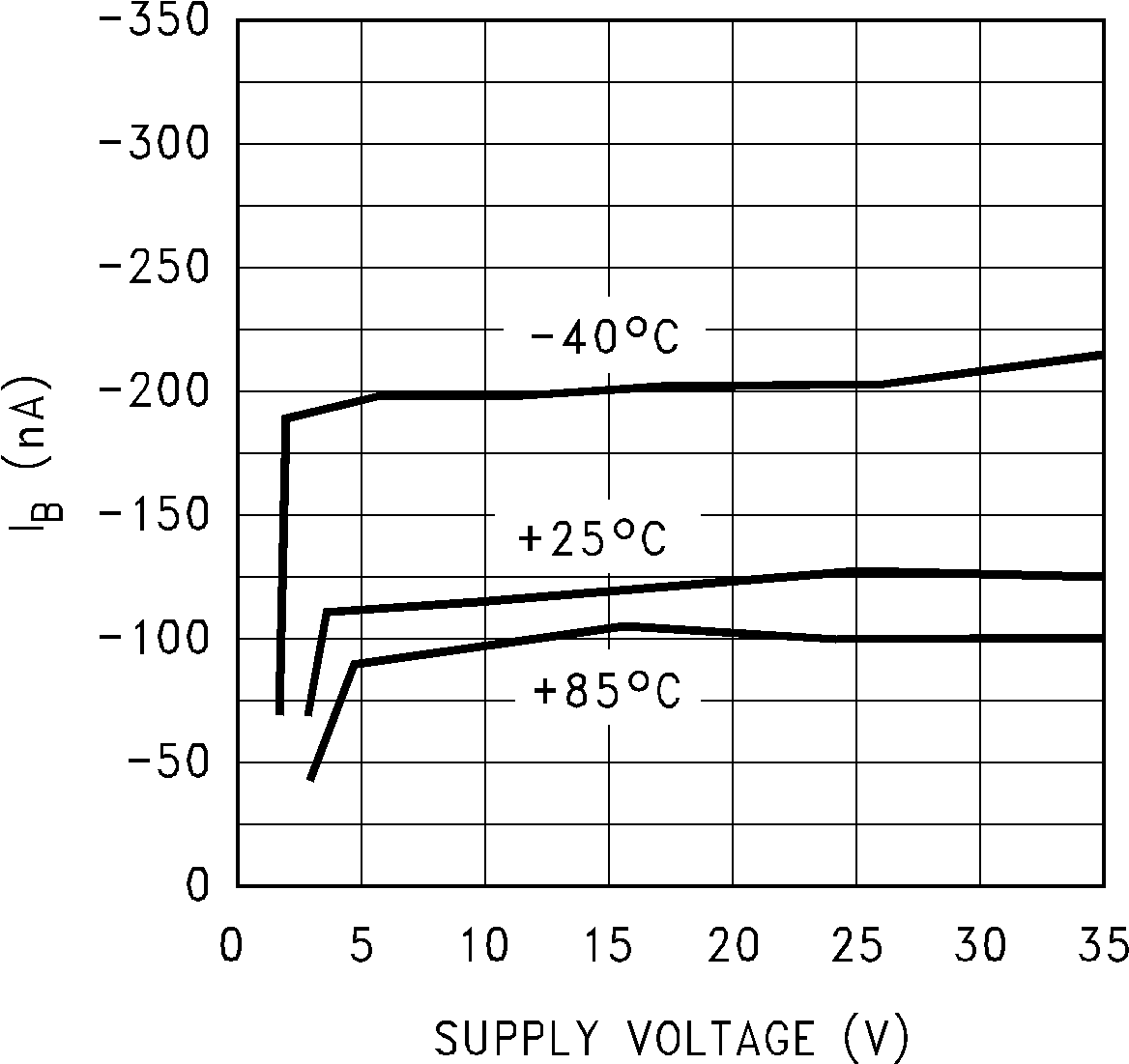
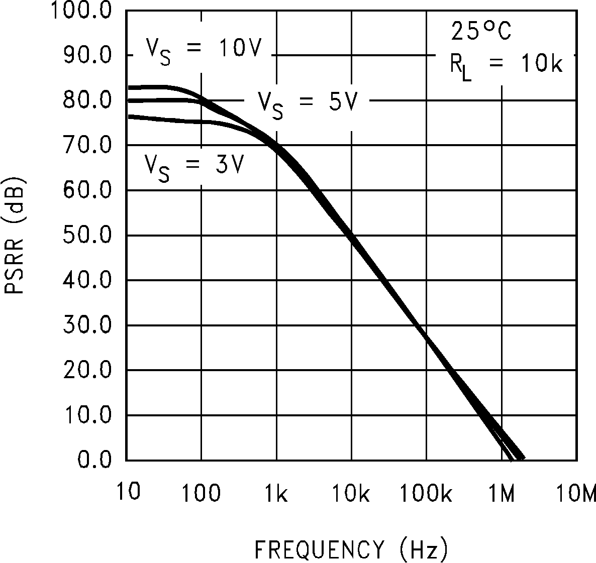
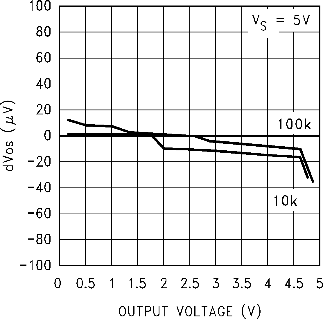
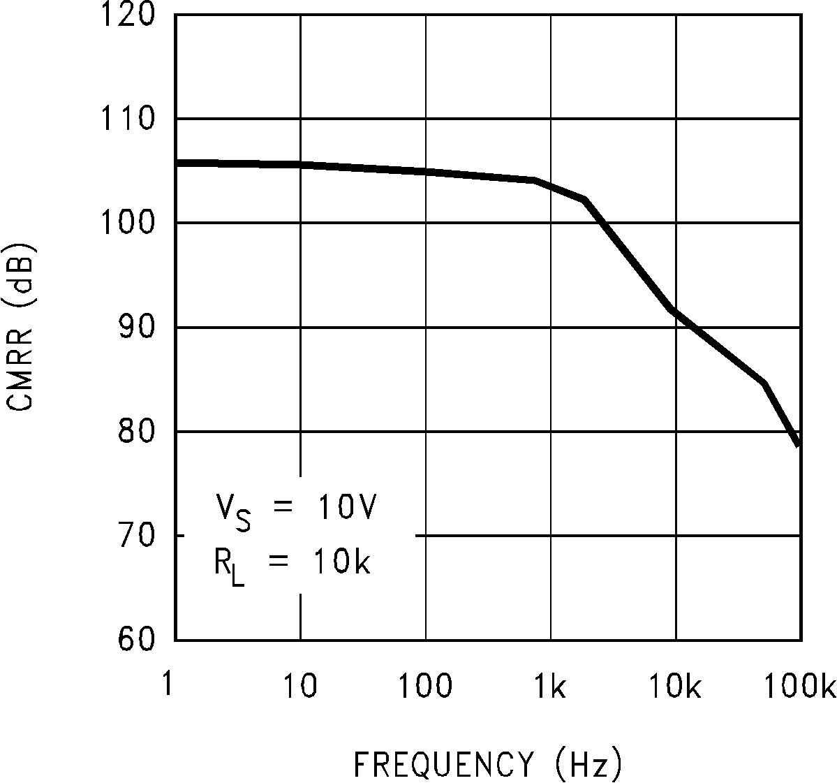
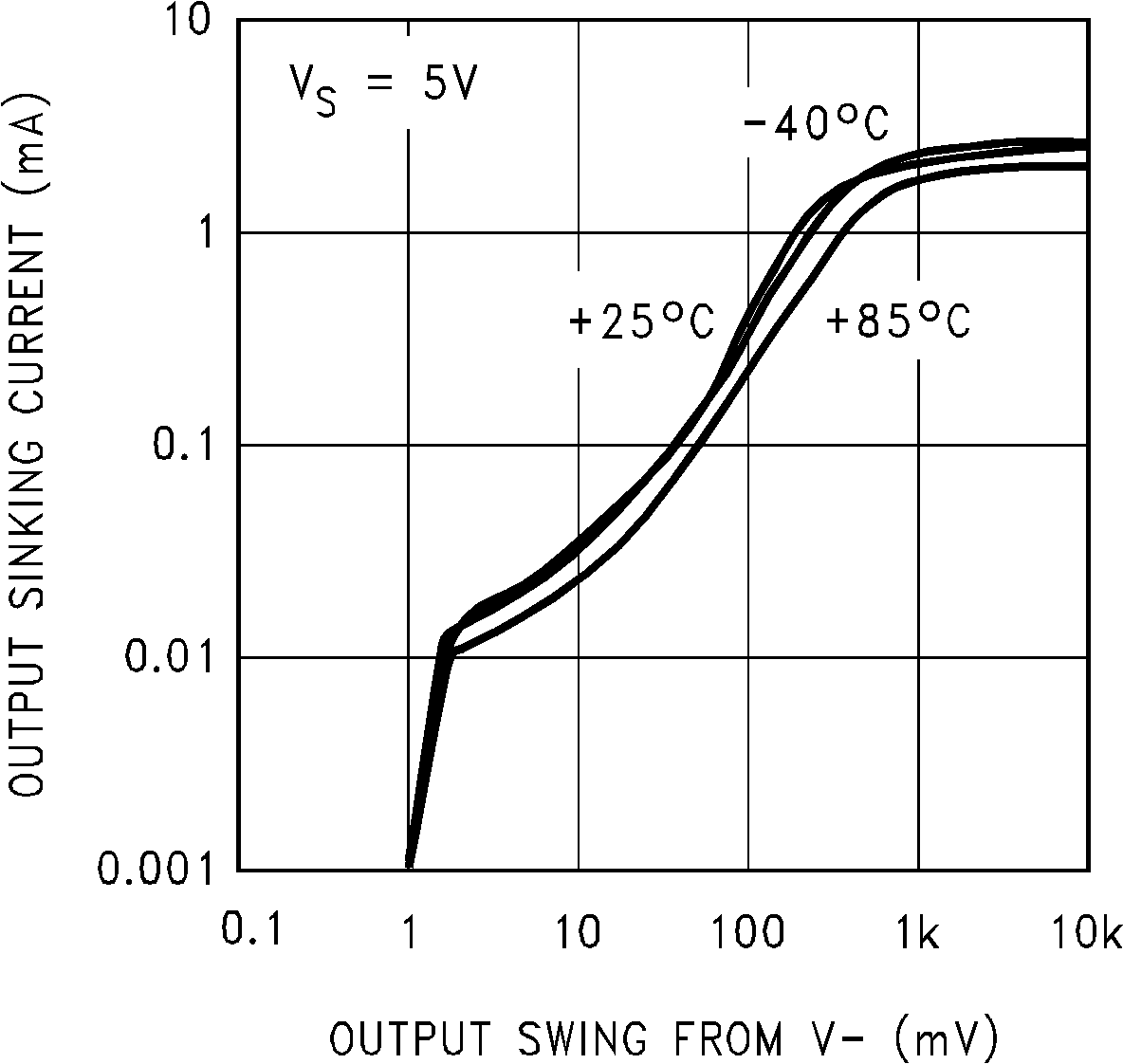
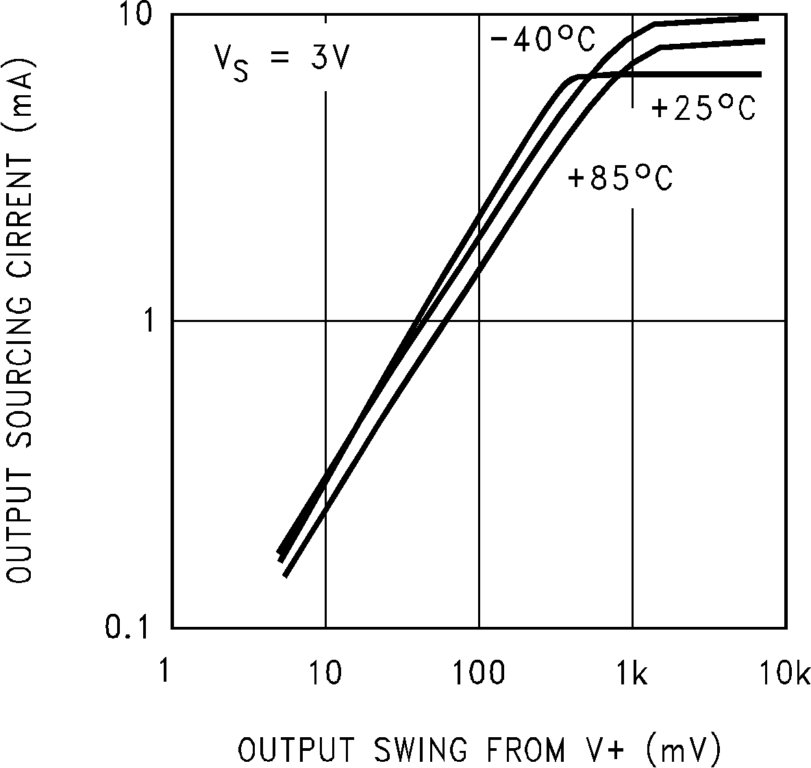
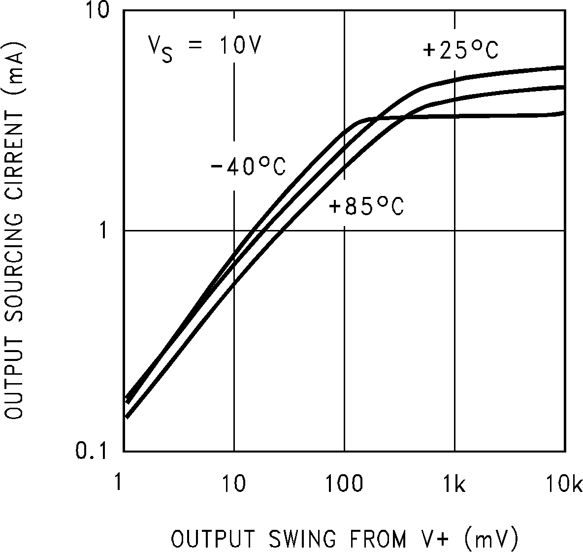
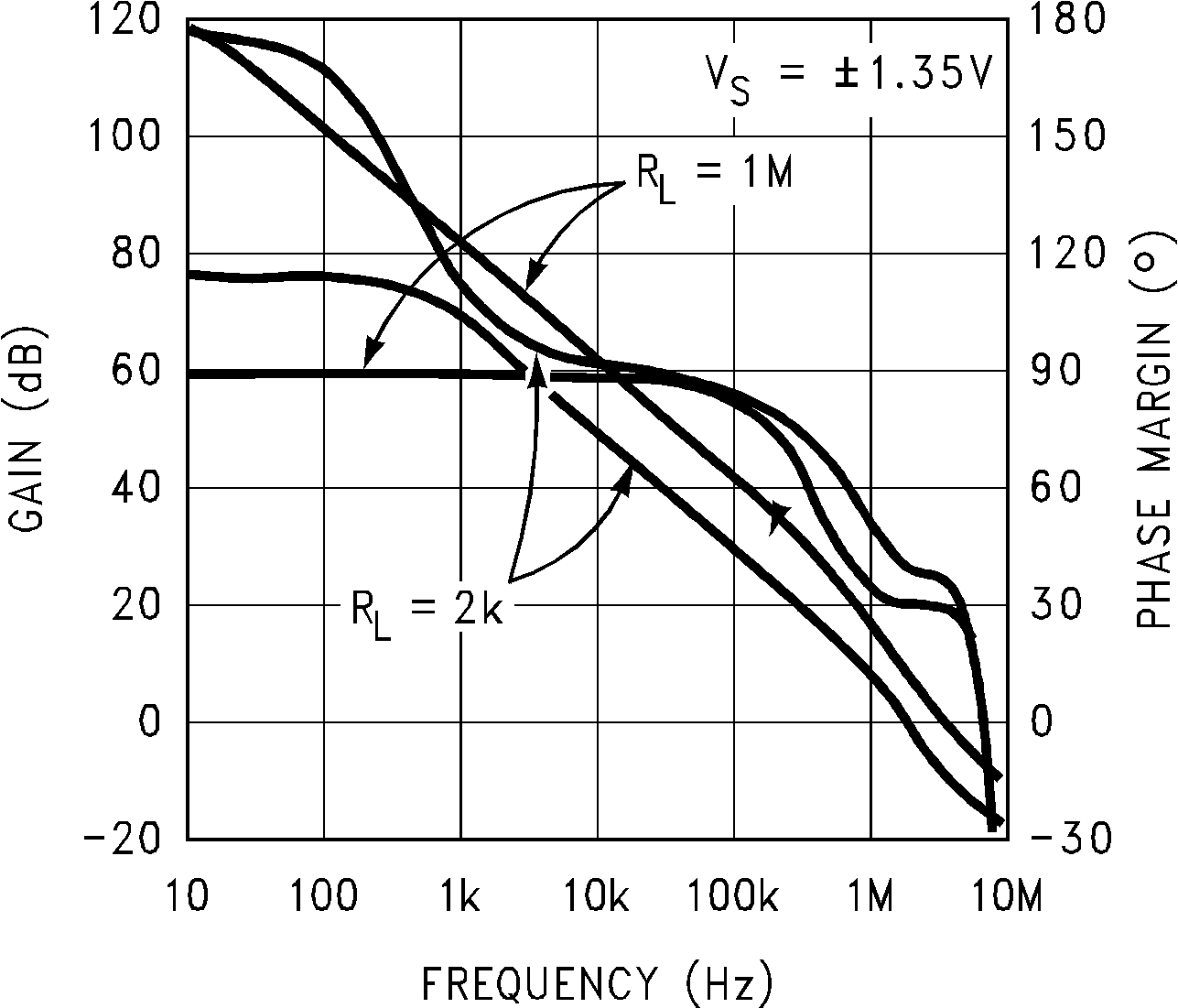
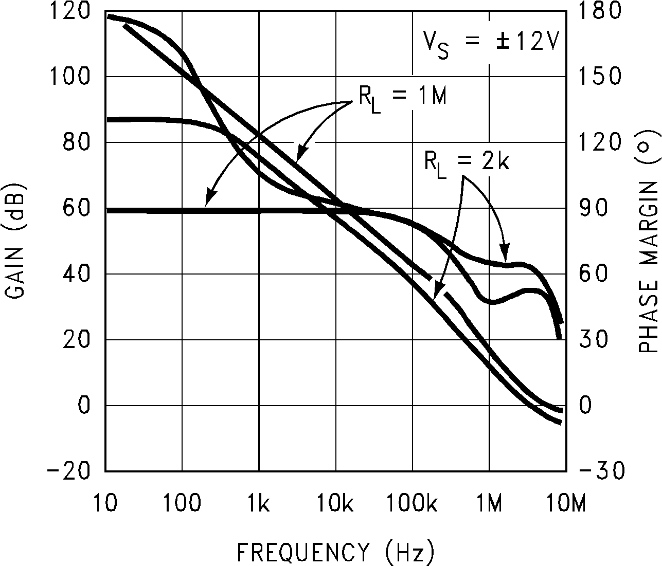
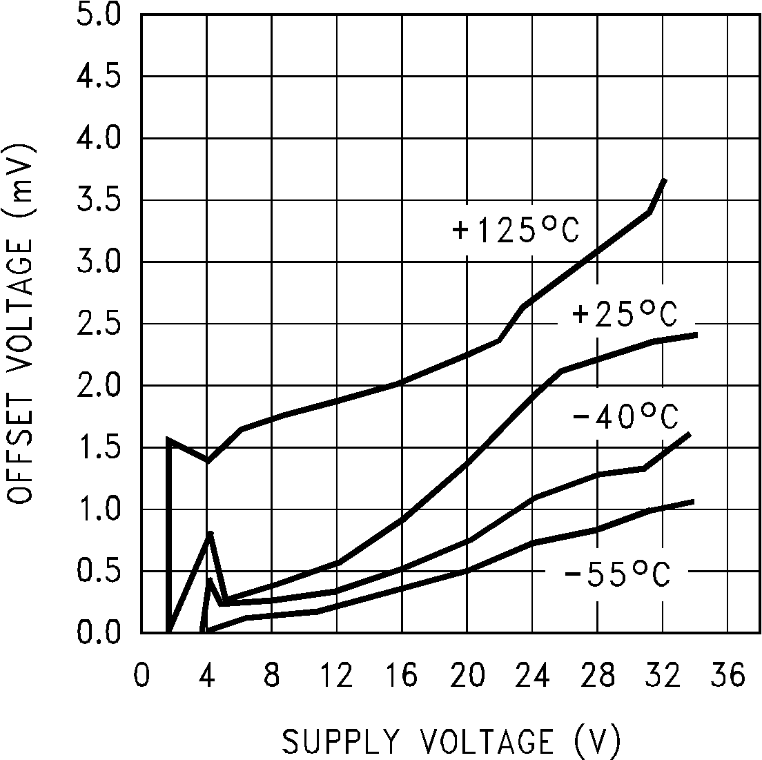
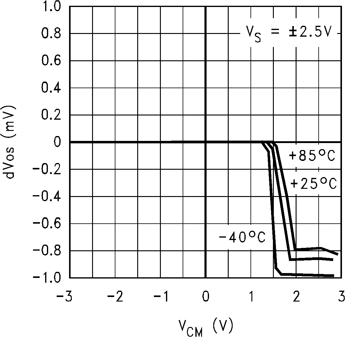
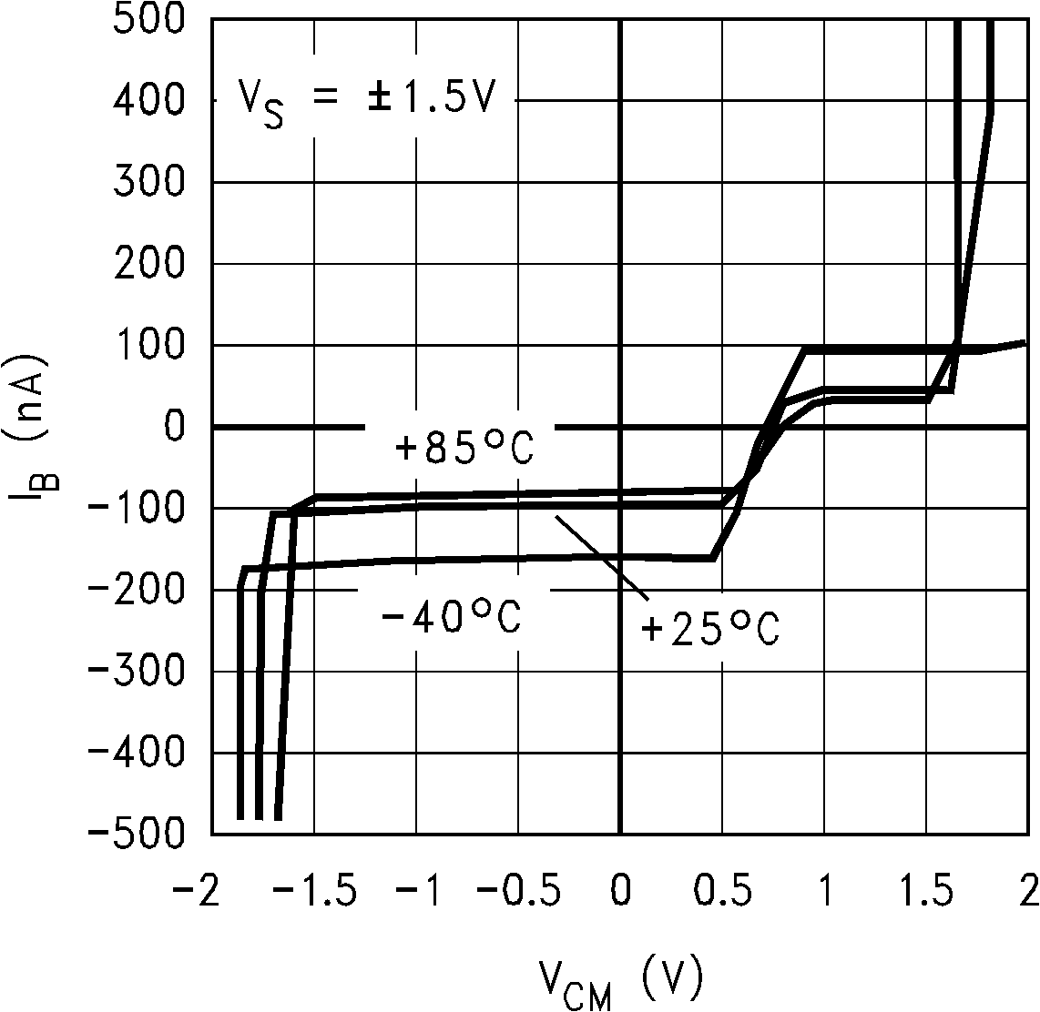
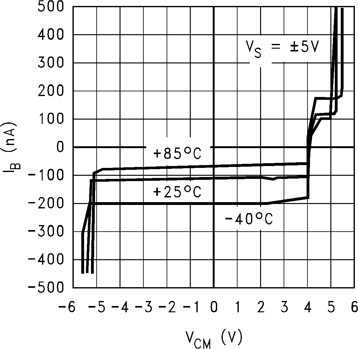
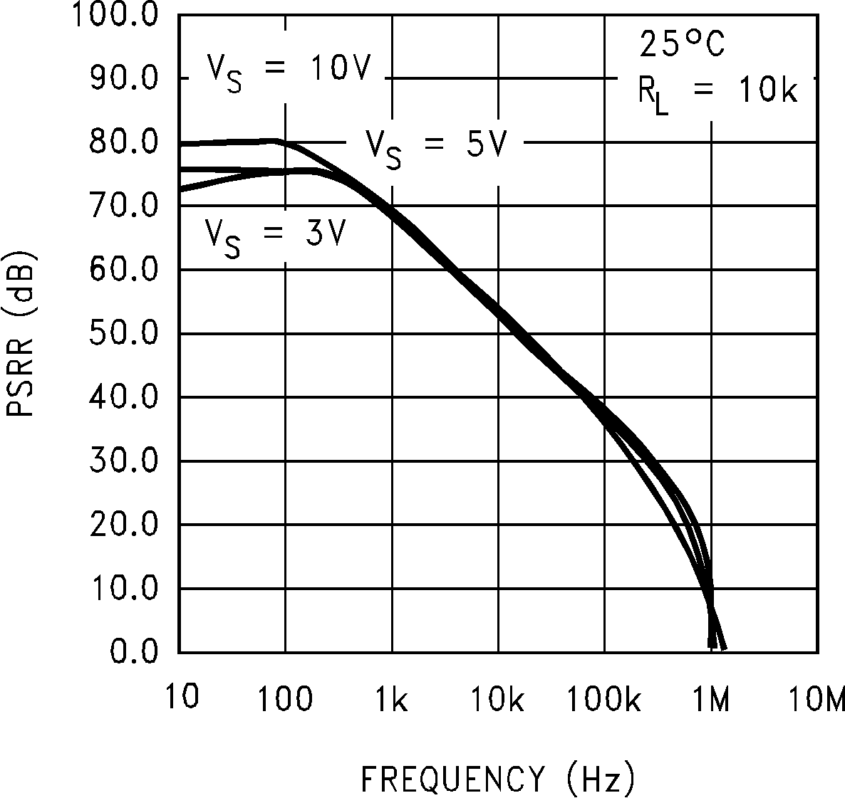
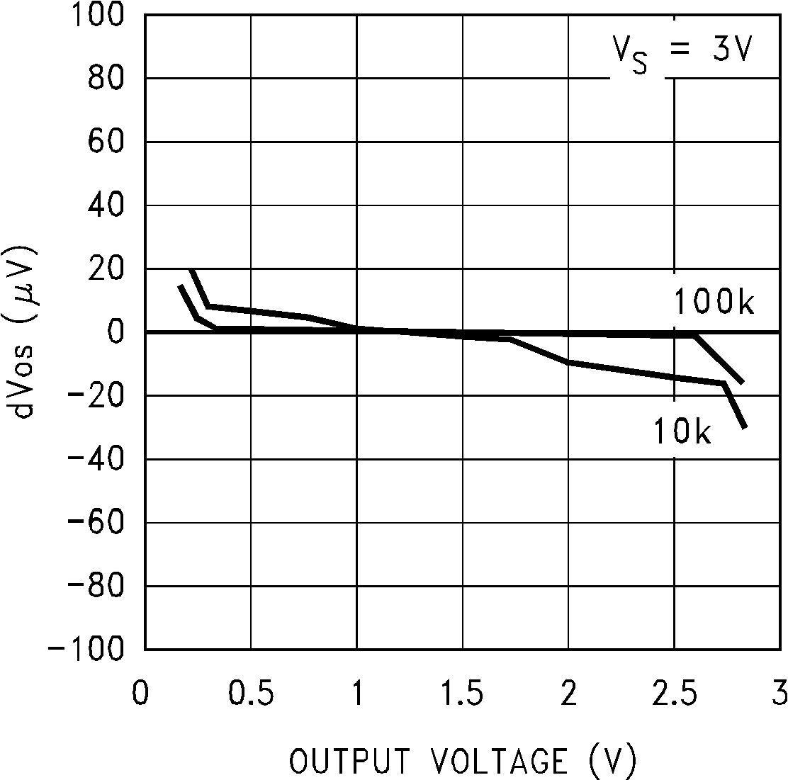
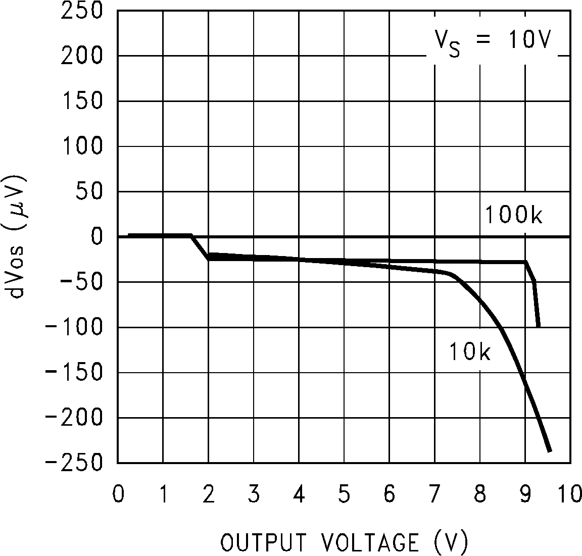
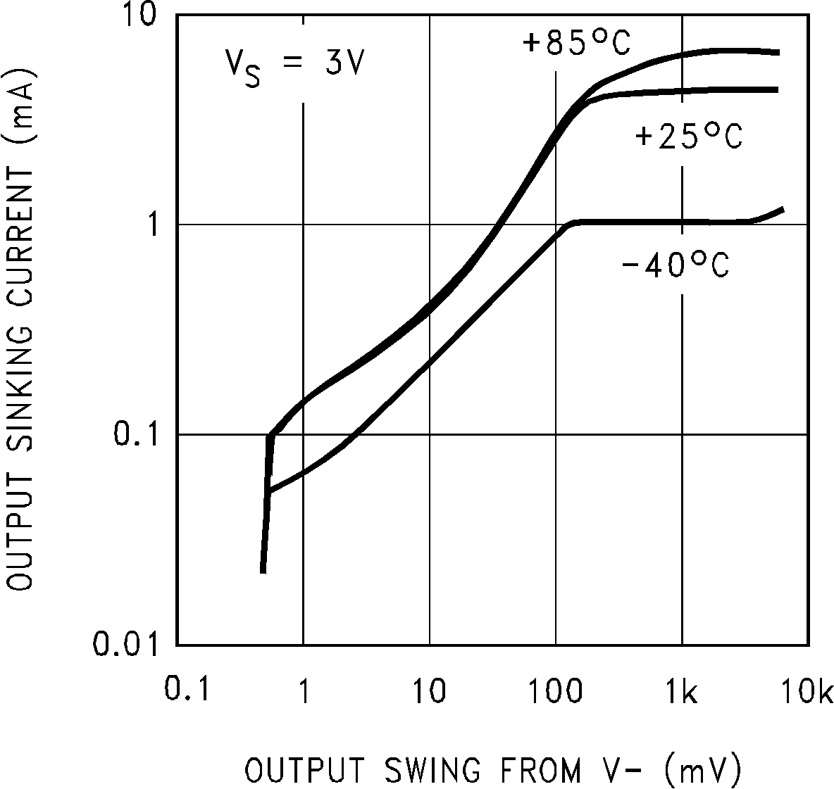
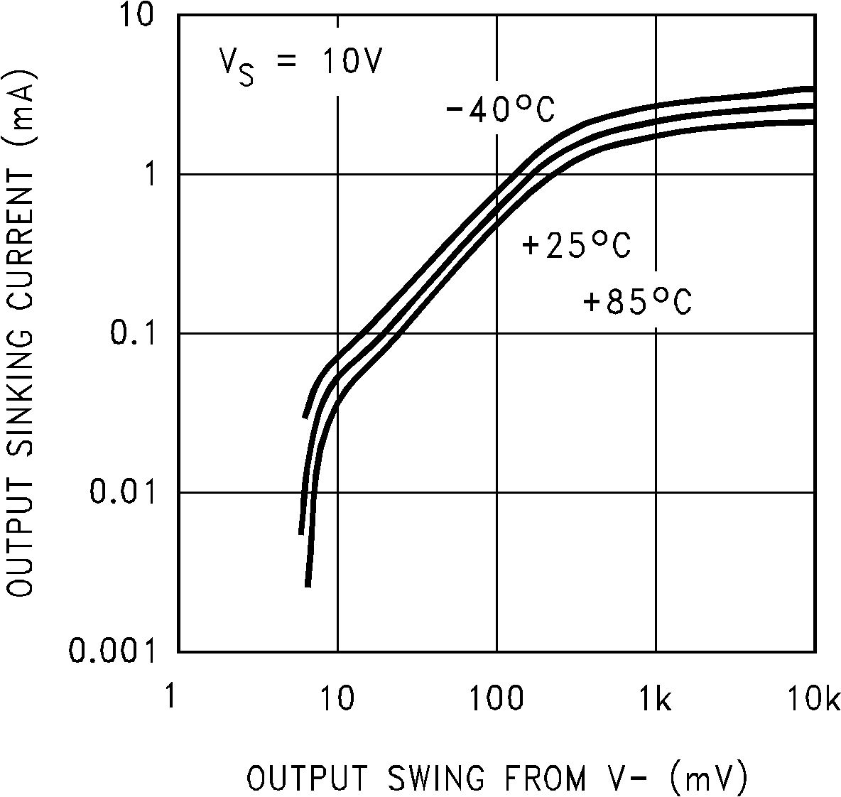
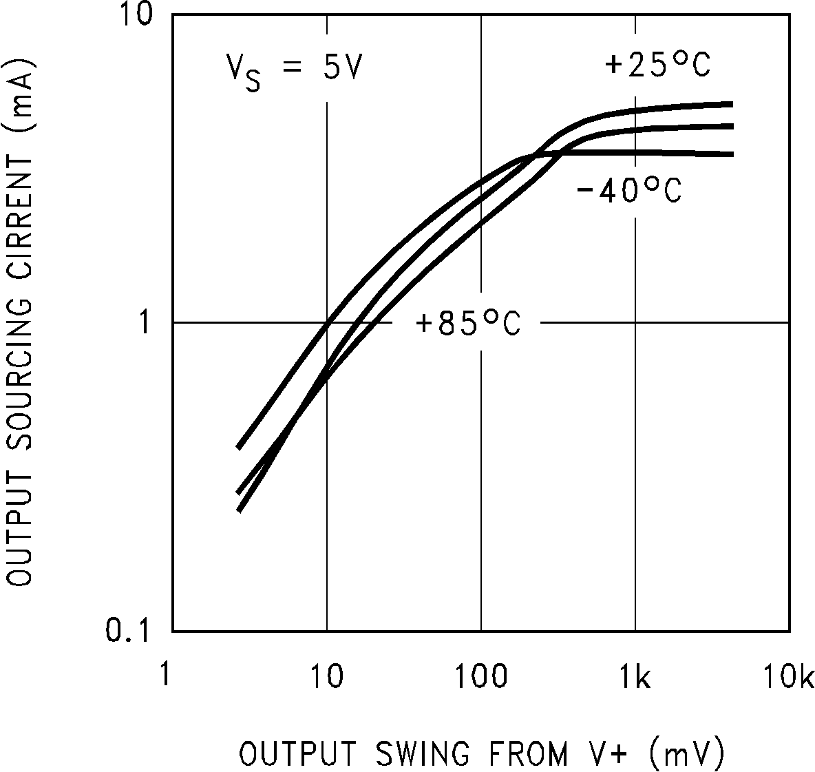
6.12 Typical Performance Characteristics
TA = 25°C, RL = 10 kΩ unless otherwise specified