SNOS751E April 2000 – September 2014 LM6132 , LM6134
PRODUCTION DATA.
- 1Features
- 2Applications
- 3Description
- 4Revision History
- 5Pin Configuration and Functions
-
6Specifications
- 6.1 Absolute Maximum Ratings
- 6.2 Handling Ratings
- 6.3 Recommended Operating Conditions
- 6.4 Thermal Information, 8-Pin
- 6.5 Thermal Information, 14-Pin
- 6.6 5.0V DC Electrical Characteristics
- 6.7 5.0V AC Electrical Characteristics
- 6.8 2.7V DC Electrical Characteristics
- 6.9 2.7V AC Electrical Characteristics
- 6.10 24V DC Electrical Characteristics
- 6.11 24V AC Electrical Characteristics
- 6.12 Typical Performance Characteristics
- 7Application and Implementation
- 8Device and Documentation Support
- 9Mechanical, Packaging, and Orderable Information
Package Options
Mechanical Data (Package|Pins)
Thermal pad, mechanical data (Package|Pins)
Orderable Information
7 Application and Implementation
7.1 Application Information
The LM6132 brings a new level of ease of use to op amp system design. Greater than rail-to-rail input voltage eliminates concern over exceeding the common-mode voltage range.
Rail-to-rail output swing provides the maximum possible dynamic range at the output. This is particularly important when operating on low supply voltages.
The high gain-bandwidth with low supply current opens new battery powered applications, where high power consumption previously reduced battery life to unacceptable levels.
To take advantage of these features, some ideas should be kept in mind, which are outlined in subsequent sections.
7.2 Enhanced Slew Rate
Unlike most bipolar op amps, the unique phase reversal prevention/speed-up circuit in the input stage eliminates phase reversal and allows the slew rate to be a function of the input signal amplitude.
Figure 30 shows how excess input signal is routed around the input collector-base junctions directly to the current mirrors.
The LM6132/34 input stage converts the input voltage change to a current change. This current change drives the current mirrors through the collectors of Q1–Q2, Q3–Q4 when the input levels are normal.
If the input signal exceeds the slew rate of the input stage and the differential input voltage rises above a diode drop, the excess signal bypasses the normal input transistors, (Q1–Q4), and is routed in correct phase through the two additional transistors, (Q5, Q6), directly into the current mirrors.
The rerouting of excess signal allows the slew-rate to increase by a factor of 10 to 1 or more. (See Figure 29).
As the overdrive increases, the op amp reacts better than a conventional op amp. Large fast pulses will raise the slew rate to around 25V to 30 V/μs.
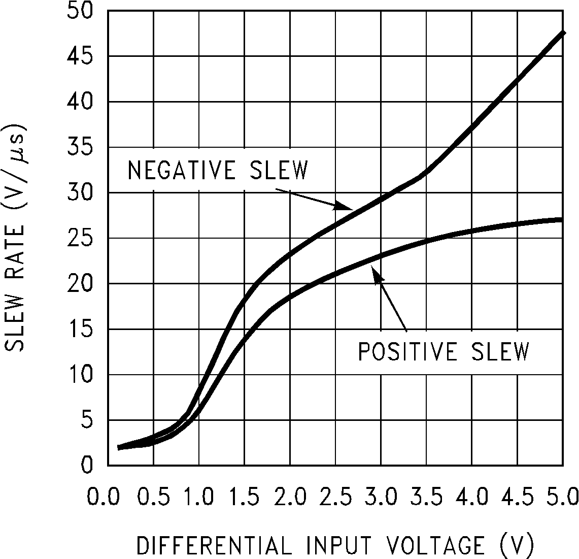 Figure 29. Slew Rate vs. Differential VIN
VS = ±12V
This effect is most noticeable at higher supply voltages and lower gains where incoming signals are likely to be large.
This speed-up action adds stability to the system when driving large capacitive loads.
7.2.1 Driving Capacitive Loads
Capacitive loads decrease the phase margin of all op amps. This is caused by the output resistance of the amplifier and the load capacitance forming an R-C phase lag network. This can lead to overshoot, ringing and oscillation. Slew rate limiting can also cause additional lag. Most op amps with a fixed maximum slew-rate will lag further and further behind when driving capacitive loads even though the differential input voltage raises. With the LM6132, the lag causes the slew rate to raise. The increased slew-rate keeps the output following the input much better. This effectively reduces phase lag. After the output has caught up with the input, the differential input voltage drops down and the amplifier settles rapidly.
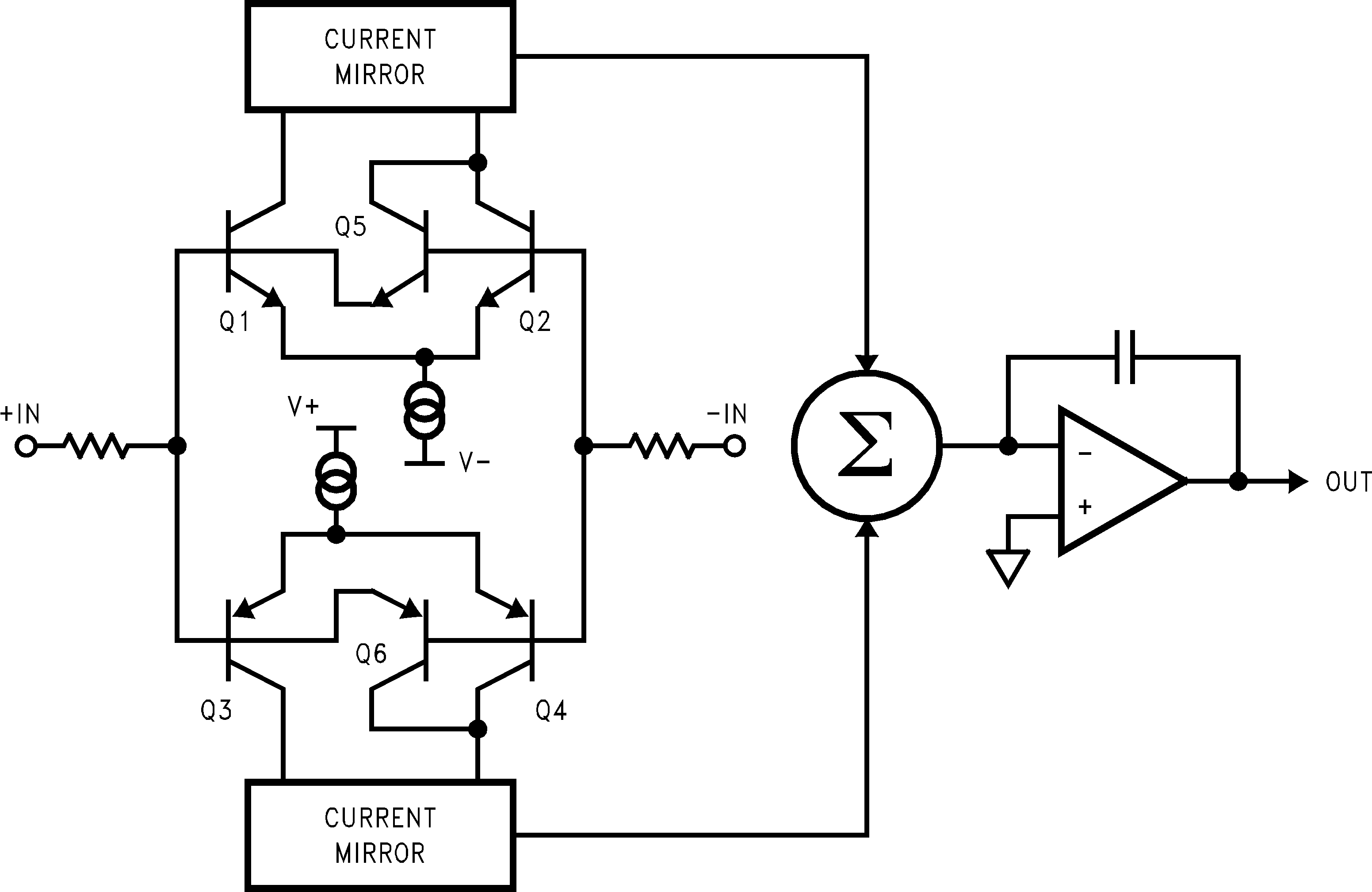 Figure 30. Internal Block Diagram
These features allow the LM6132 to drive capacitive loads as large as 500 pF at unity gain and not oscillate. The scope photos (Figure 31 and Figure 32) show the LM6132 driving a 500 pF load. In Figure 31 , the lower trace is with no capacitive load and the upper trace is with a 500 pF load. Here we are operating on ±12V supplies with a 20 VPP pulse. Excellent response is obtained with a Cf of 39 pF. In Figure 32, the supplies have been reduced to ±2.5V, the pulse is 4 VPP and CF is 39 pF. The best value for the compensation capacitor should be established after the board layout is finished because the value is dependent on board stray capacity, the value of the feedback resistor, the closed loop gain and, to some extent, the supply voltage.
Another effect that is common to all op amps is the phase shift caused by the feedback resistor and the input capacitance. This phase shift also reduces phase margin. This effect is taken care of at the same time as the effect of the capacitive load when the capacitor is placed across the feedback resistor.
The circuit shown in Figure 33 was used for Figure 31 and Figure 32.
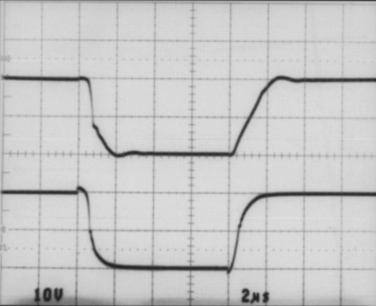 Figure 31. Twenty-Volt Step Response:
with Cap Load (Top Trace)
without Cap Load (Bottom Trace)
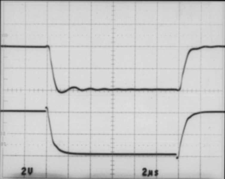 Figure 32. Four-Volt Step Response:
with Cap Load (Top Trace)
without Cap Load (Bottom Trace)
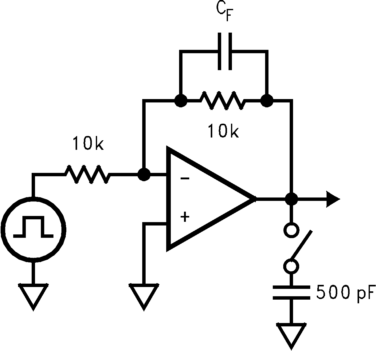 Figure 33. Cap Load Test Circuit
Figure 34 shows a method for compensating for load capacitance (CO) effects by adding both an isolation resistor RO at the output and a feedback capacitor CFdirectly between the output and the inverting input pin. Feedback capacitor CF compensates for the pole introduced by RO and CO, minimizing ringing in the output waveform while the feedback resistor RF compensates for dc inaccuracies introduced by RO. Depending on the size of the load capacitance, the value of ROis typically chosen to be between 100 Ω to 1 kΩ.
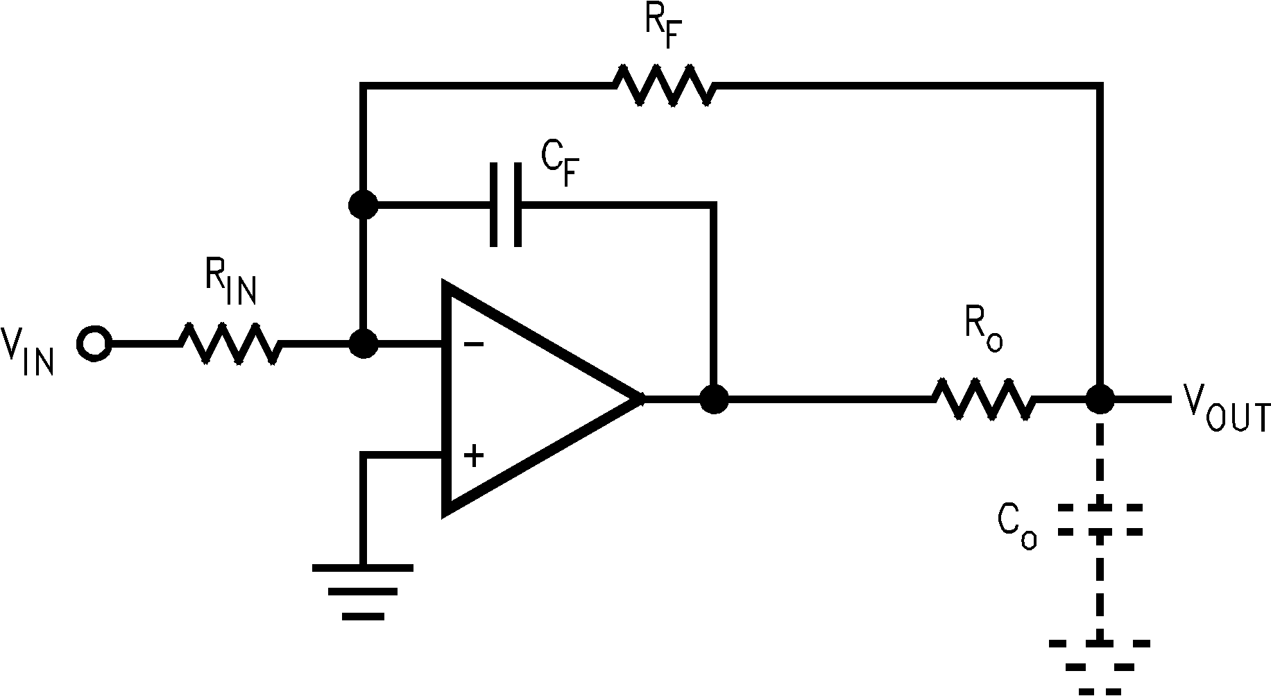 Figure 34. Capacitive Loading Compensation Technique
7.3 Typical Applications
7.3.1 Three Op Amp Instrumentation Amp with Rail-to-Rail Input and Output
Using the LM6134, a 3 op amp instrumentation amplifier with rail-to-rail inputs and rail to rail output can be made. These features make these instrumentation amplifiers ideal for single supply systems.
Some manufacturers use a precision voltage divider array of 5 resistors to divide the common-mode voltage to get an input range of rail-to-rail or greater. The problem with this method is that it also divides the signal, so to even get unity gain, the amplifier must be run at high closed loop gains. This raises the noise and drift by the internal gain factor and lowers the input impedance. Any mismatch in these precision resistors reduces the CMR as well. Using the LM6134, all of these problems are eliminated.
In this example, amplifiers A and B act as buffers to the differential stage (Figure 35). These buffers assure that the input impedance is over 100 MΩ and they eliminate the requirement for precision matched resistors in the input stage. They also assure that the difference amp is driven from a voltage source. This is necessary to maintain the CMR set by the matching of R1–R2 with R3–R4.
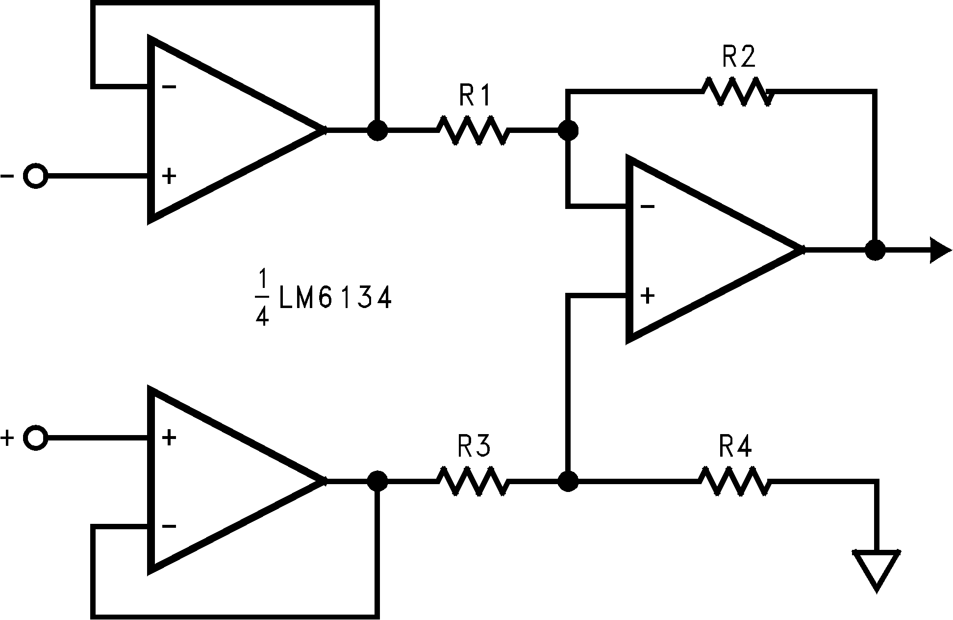 Figure 35. Instrumentation Amplifier
7.3.2 Flat Panel Display Buffering
Three features of the LM6132/34 make it a superb choice for TFT LCD applications. First, its low current draw (360 μA per amplifier at 5 V) makes it an ideal choice for battery powered applications such as in laptop computers. Second, since the device operates down to 2.7 V, it is a natural choice for next generation 3V TFT panels. Last, but not least, the large capacitive drive capability of the LM6132 comes in very handy in driving highly capacitive loads that are characteristic of LCD display drivers.
The large capacitive drive capability of the LM6132/34 allows it to be used as buffers for the gamma correction reference voltage inputs of resistor-DAC type column (Source) drivers in TFT LCD panels. This amplifier is also useful for buffering only the center reference voltage input of Capacitor-DAC type column (Source) drivers such as the LMC750X series.
Since for VGA and SVGA displays, the buffered voltages must settle within approximately 4 μs, the well known technique of using a small isolation resistor in series with the amplifier's output very effectively dampens the ringing at the output.
With its wide supply voltage range of 2.7 V to 24 V, the LM6132/34 can be used for a diverse range of applications. The system designer is thus able to choose a single device type that serves many sub-circuits in the system, eliminating the need to specify multiple devices in the bill of materials. Along with its sister parts, the LM6142 and LM6152 that have the same wide supply voltage capability, choice of the LM6132 in a design eliminates the need to search for multiple sources for new designs.