SNVSBZ4A February 2020 – November 2021 LM61480 , LM61495 , LM62460
PRODUCTION DATA
- 1 Features
- 2 Applications
- 3 Description
- 4 Revision History
- 5 Device Comparison Table
- 6 Pin Configuration and Functions
- 7 Specifications
-
8 Detailed Description
- 8.1 Overview
- 8.2 Functional Block Diagram
- 8.3
Feature Description
- 8.3.1 Output Voltage Selection
- 8.3.2 Enable EN Pin and Use as VIN UVLO
- 8.3.3 SYNC/MODE Uses for Synchronization
- 8.3.4 Clock Locking
- 8.3.5 Adjustable Switching Frequency
- 8.3.6 RESET Output Operation
- 8.3.7 Internal LDO, VCC UVLO, and BIAS Input
- 8.3.8 Bootstrap Voltage and VCBOOT-UVLO (CBOOT Pin)
- 8.3.9 Adjustable SW Node Slew Rate
- 8.3.10 Spread Spectrum
- 8.3.11 Soft Start and Recovery From Dropout
- 8.3.12 Overcurrent and Short Circuit Protection
- 8.3.13 Hiccup
- 8.3.14 Thermal Shutdown
- 8.4 Device Functional Modes
-
9 Application and Implementation
- 9.1 Application Information
- 9.2
Typical Application
- 9.2.1 Design Requirements
- 9.2.2
Detailed Design Procedure
- 9.2.2.1 Choosing the Switching Frequency
- 9.2.2.2 Setting the Output Voltage
- 9.2.2.3 Inductor Selection
- 9.2.2.4 Output Capacitor Selection
- 9.2.2.5 Input Capacitor Selection
- 9.2.2.6 BOOT Capacitor
- 9.2.2.7 BOOT Resistor
- 9.2.2.8 VCC
- 9.2.2.9 CFF and RFF Selection
- 9.2.2.10 RSPSP Selection
- 9.2.2.11 RT Selection
- 9.2.2.12 RMODE Selection
- 9.2.2.13 External UVLO
- 9.2.2.14 Maximum Ambient Temperature
- 9.2.3 Application Curves
- 10Power Supply Recommendations
- 11Layout
- 12Device and Documentation Support
- 13Mechanical, Packaging, and Orderable Information
Package Options
Mechanical Data (Package|Pins)
- RPH|16
Thermal pad, mechanical data (Package|Pins)
- RPH|16
Orderable Information
9.2.2.14 Maximum Ambient Temperature
As with any power conversion device, the LM6x4xx dissipates internal power while operating. The effect of this power dissipation is to raise the internal temperature of the converter above ambient temperature. The internal die temperature (TJ) is a function of the following:
- Ambient temperature
- Power loss
- Effective thermal resistance, RθJA of the device
- PCB layout
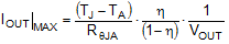
where
- η = efficiency
- TA = ambient temperature
- TJ = junction temperature
- RθJA = the effective thermal resistance of the IC junction to the air, mainly through the PCB
The effective RθJA is a critical parameter and depends on many factors (just to mention a few of the most critical parameters:
- Power dissipation
- Air temperature
- Airflow
- PCB area
- Copper heat-sink area
- Number of thermal vias under or near the package
- Adjacent component placement
| VIN = 13.5 V | VOUT = 5 V | |
| ƒSW = 400 kHz | RθJA = 22°C/W |
| VIN = 13.5 V | VOUT = 5 V | |
| ƒSW = 2.2 MHz | RθJA = 22°C/W |
Use the following resources as a guide to optimal thermal PCB design and estimating RθJA for a given application environment: