SNVSBZ4A February 2020 – November 2021 LM61480 , LM61495 , LM62460
PRODUCTION DATA
- 1 Features
- 2 Applications
- 3 Description
- 4 Revision History
- 5 Device Comparison Table
- 6 Pin Configuration and Functions
- 7 Specifications
-
8 Detailed Description
- 8.1 Overview
- 8.2 Functional Block Diagram
- 8.3
Feature Description
- 8.3.1 Output Voltage Selection
- 8.3.2 Enable EN Pin and Use as VIN UVLO
- 8.3.3 SYNC/MODE Uses for Synchronization
- 8.3.4 Clock Locking
- 8.3.5 Adjustable Switching Frequency
- 8.3.6 RESET Output Operation
- 8.3.7 Internal LDO, VCC UVLO, and BIAS Input
- 8.3.8 Bootstrap Voltage and VCBOOT-UVLO (CBOOT Pin)
- 8.3.9 Adjustable SW Node Slew Rate
- 8.3.10 Spread Spectrum
- 8.3.11 Soft Start and Recovery From Dropout
- 8.3.12 Overcurrent and Short Circuit Protection
- 8.3.13 Hiccup
- 8.3.14 Thermal Shutdown
- 8.4 Device Functional Modes
-
9 Application and Implementation
- 9.1 Application Information
- 9.2
Typical Application
- 9.2.1 Design Requirements
- 9.2.2
Detailed Design Procedure
- 9.2.2.1 Choosing the Switching Frequency
- 9.2.2.2 Setting the Output Voltage
- 9.2.2.3 Inductor Selection
- 9.2.2.4 Output Capacitor Selection
- 9.2.2.5 Input Capacitor Selection
- 9.2.2.6 BOOT Capacitor
- 9.2.2.7 BOOT Resistor
- 9.2.2.8 VCC
- 9.2.2.9 CFF and RFF Selection
- 9.2.2.10 RSPSP Selection
- 9.2.2.11 RT Selection
- 9.2.2.12 RMODE Selection
- 9.2.2.13 External UVLO
- 9.2.2.14 Maximum Ambient Temperature
- 9.2.3 Application Curves
- 10Power Supply Recommendations
- 11Layout
- 12Device and Documentation Support
- 13Mechanical, Packaging, and Orderable Information
Package Options
Mechanical Data (Package|Pins)
- RPH|16
Thermal pad, mechanical data (Package|Pins)
- RPH|16
Orderable Information
3 Description
The LM6x4xx family of buck regulators are regulators that provide either fixed or adjustable output voltage that can be set from 1 V to 95% of expected input voltage. These regulators operate under a wide input voltage range or 3 V to 36 V and have transient tolerance up to 42 V.
The family is designed for low EMI. The devices incorporate pin-selectable spread spectrum and an adjustable SW node rise time. Dual Random Spread Spectrum (DRSS) frequency hopping is set to ±5.5% (typical), drastically reducing peak emissions through a combination of triangular and pseudo random modulation. DRSS also includes advanced techniques to reduce output voltage ripple caused by spread spectrum modulation.
An open-drain RESET output with filtering and delayed release gives a true indication of system status. In auto mode, the device automatically transitions between fixed-frequency pulse width modulation (FPWM) and pulse frequency modulation (PFM) modes of operation, allowing an unloaded current consumption of only 5 µA (typical). Electrical characteristics are specified over a junction temperature range of –40°C to +150°C.
| PART NUMBER | PACKAGE(1) | BODY SIZE (NOM) |
|---|---|---|
| LM61495 | VQFN (16) | 4.50 mm × 3.50 mm |
| LM61480 | ||
| LM62460 |
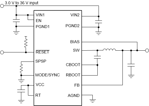
 Simplified Schematic
VOUT = 5 V, FSW = 0.4 MHz