SNOSAV4B April 2008 – January 2016 LM7332
PRODUCTION DATA.
- 1 Features
- 2 Applications
- 3 Description
- 4 Revision History
- 5 Pin Configuration and Functions
- 6 Specifications
- 7 Detailed Description
- 8 Application and Implementation
- 9 Power Supply Recommendations
- 10Layout
- 11Device and Documentation Support
- 12Mechanical, Packaging, and Orderable Information
Package Options
Mechanical Data (Package|Pins)
Thermal pad, mechanical data (Package|Pins)
Orderable Information
7 Detailed Description
7.1 Overview
The LM7332 device is a rail-to-rail input and output amplifier with wide operating voltages and high-output currents. The LM7322 is efficient, achieving 15.2-V/µs slew rate and 21-MHz unity gain bandwidth while requiring only 2 mA of total supply current. The LM7332 device performance is fully specified for operation at 5 V, ±5 V and ±15 V.
The LM7332 device is designed to drive unlimited capacitive loads without oscillations. The LM7332 is fully tested at −40°C, 125°C, and 25°C, with modern automatic test equipment. High performance from −40°C to +125°C, detailed specifications, and extensive testing makes them suitable for industrial, automotive, and communications applications.
Most device parameters are insensitive to power supply voltage, and this makes the parts easier to use where supply voltage may vary, such as automotive electrical systems and battery-powered equipment. The LM7332 has a true rail-to-rail output and can supply a respectable amount of current (±70 mA) with minimal head room from either rail (1 V).
7.2 Functional Block Diagram

7.3 Feature Description
7.3.1 Estimating the Output Voltage Swing
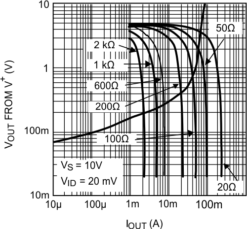
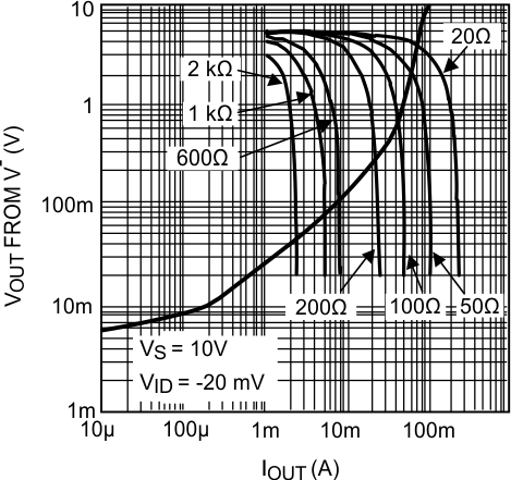
It is important to keep in mind that the steady-state output current will be less than the current available when there is an input overdrive present. For steady-state conditions, Figure 47 and Figure 48 plots can be used to predict the output swing. These plots also show several load lines corresponding to loads tied between the output and ground. In each case, the intersection of the device plot at the appropriate temperature with the load line would be the typical output swing possible for that load. For example, a 600-Ω load can accommodate an output swing to within 100 mV of V− and to 250 mV of V+ (VS = ±5 V) corresponding to a typical 9.65-VPP unclipped swing.
 Figure 47. Steady-State Output Sourcing Characteristics With Load Lines
 Figure 48. Steady-State Output Sinking Characteristics With Load Lines
7.4 Device Functional Modes
7.4.1 Driving Capacitive Loads
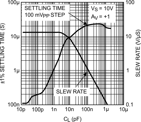
The LM7332 is specifically designed to drive unlimited capacitive loads without oscillations as shown in Figure 49.
 Figure 49. Settling Time and Slew Rate vs Capacitive Load
In addition, the output current handling capability of the device allows for good slewing characteristics even with large capacitive loads as shown in Figure 49. The combination of these features is ideal for applications such as TFT flat panel buffers, A/D converter input amplifiers and power transistor driver.
However, as in most operational amplifiers, addition of a series isolation resistor between the operational amplifier and the capacitive load improves the settling and overshoot performance.
Output current drive is an important parameter when driving capacitive loads. This parameter will determine how fast the output voltage can change. Referring to Figure 49, two distinct regions can be identified. Below about 10,000 pF, the output slew rate is solely determined by the compensation capacitor value of the operational amplifier and available current into that capacitor. Beyond 10 nF, the slew rate is determined by the available output current of the operational amplifier. An estimate of positive and negative slew rates for loads larger than 100 nF can be made by dividing the short circuit current value by the capacitor.
7.4.2 Output Voltage Swing Close to V−
The output stage design of the LM7332 allows voltage swings to within millivolts of either supply rail for maximum flexibility and improved useful range. Because of this design architecture, with output approaching either supply rail, the output transistor collector-base junction reverse bias decreases. With output less than a Vbe from either rail, the corresponding output transistor operates near saturation. In this mode of operation, the transistor exhibits higher junction capacitance and lower ft which reduces phase margin. With the Noise Gain (NG = 1 + RF/RG, RF and RG are external gain setting resistors) of 2 or higher, there is sufficient phase margin that this reduction in phase margin is of no consequence. However, with lower Noise Gain (<2) and with less than 150 mV to the supply rail, if the output loading is light, the phase margin reduction could result in unwanted oscillations.
In the case of the LM7332, due to inherent architectural specifics, the oscillation occurs only with respect to the output transistor at V− when output swings to within 150 mV of V−. However, if this output transistor's collector current is larger than its idle value of a few microamps, the phase margin loss becomes insignificant. In this case, 300 μA is the required collector current of the output transistor to remedy this situation. Therefore, when all the aforementioned critical conditions are present at the same time (NG < 2, VOUT < 150 mV from supply rails and output load is light) it is possible to ensure stability by adding a load resistor to the output to provide the output transistor the necessary minimum collector current (300 μA).
For 12-V (or ±6-V) operation, for example, add a 39-kΩ resistor from the output to V+ to cause 300-µA output sinking current and ensure stability. This is equivalent to about 15% increase in total quiescent power dissipation.