SLVSEM1A March 2019 – September 2019 LM76202-Q1
PRODUCTION DATA.
- 1 Features
- 2 Applications
- 3 Description
- 4 Revision History
- 5 Pin Configuration and Functions
- 6 Specifications
- 7 Parameter Measurement Information
-
8 Detailed Description
- 8.1 Overview
- 8.2 Functional Block Diagram
- 8.3
Feature Description
- 8.3.1 Undervoltage Lockout (UVLO)
- 8.3.2 Overvoltage Protection (OVP)
- 8.3.3 Reverse Battery Protection
- 8.3.4 Hot Plug-In and In-Rush Current Control
- 8.3.5 Overload and Short Circuit Protection
- 8.4 Device Functional Modes
-
9 Application and Implementation
- 9.1 Application Information
- 9.2
Typical Application
- 9.2.1 Design Requirements
- 9.2.2 Detailed Design Procedure
- 9.2.3 Application Curves
- 10Power Supply Recommendations
- 11Layout
- 12Device and Documentation Support
- 13Mechanical, Packaging, and Orderable Information
Package Options
Mechanical Data (Package|Pins)
- PWP|16
Thermal pad, mechanical data (Package|Pins)
- PWP|16
Orderable Information
8.3.1 Undervoltage Lockout (UVLO)
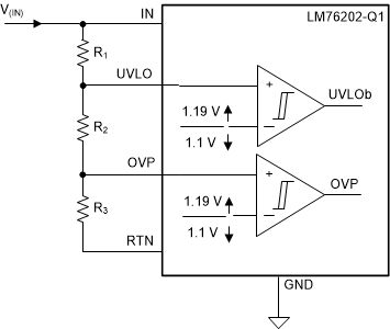
This section describes the undervoltage comparator input. When the voltage at UVLO pin falls below V(UVLOF) during input power fail or input undervoltage fault, the internal FET quickly turns off and FLT is asserted. The UVLO comparator has a hysteresis of 90 mV. To set the input UVLO threshold, connect a resistor divider network from IN supply to UVLO terminal to RTN as shown in Figure 20.
 Figure 20. UVLO and OVP Thresholds Set by R1, R2 and R3
 If the undervoltage lockout (UVLO) function is not needed, the UVLO terminal must be connected to the IN terminal. UVLO terminal must not be left floating.
The device also implements an internal power ON reset (POR) function on the IN terminal. The device disables the internal circuitry when the IN terminal voltage falls below internal POR threshold V(PORF). The internal POR threshold has a hysteresis of 275 mV.