SLOS481B July 2010 – October 2014 LM833
PRODUCTION DATA.
- 1 Features
- 2 Applications
- 3 Description
- 4 Typical Design Example Audio Pre-Amplifier
- 5 Revision History
- 6 Pin Configuration and Functions
- 7 Specifications
- 8 Detailed Description
- 9 Application and Implementation
- 10Power Supply Recommendations
- 11Layout
- 12Device and Documentation Support
- 13Mechanical, Packaging, and Orderable Information
Package Options
Mechanical Data (Package|Pins)
Thermal pad, mechanical data (Package|Pins)
Orderable Information
9 Application and Implementation
NOTE
Information in the following applications sections is not part of the TI component specification, and TI does not warrant its accuracy or completeness. TI’s customers are responsible for determining suitability of components for their purposes. Customers should validate and test their design implementation to confirm system functionality.
9.1 Application Information
An application of the LM833 is the two stage RIAA Phono Preamplifier. A primary task of the phono preamplifier is to provide gain (usually 30 to 40 dB at 1 kHz) and accurate amplitude and phase equalization to the signal from a moving magnet or a moving coil cartridge. In addition to the amplification and equalization functions, the phono preamp must not add significant noise or distortion to the signal from the cartridge. The circuit shown in Figure 36 uses two amplifiers, fulfills these qualifications, and has greatly improved performance over a single-amplifier design.
9.2 Typical Application
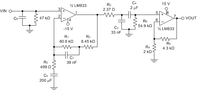 Figure 36. RIAA Phono Preamplifier
9.2.1 Design Requirements
- Supply Voltage = ±15 V
- Low-Frequency −3 dB corner of the first amplifier (f0) > 20 Hz (below audible range)
- Low-Frequency −3 dB corner of the second stage (fL) = 20.2 Hz
9.2.2 Detailed Design Procedure
9.2.2.1 Introduction to Design Method
Equation 1 through Equation 5 show the design equations for the preamplifier.
where
- A1 is the 1 kHz voltage gain of the first amplifier
where
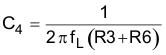
- fL is the low-frequency −3 dB corner of the second stage
For standard RIAA preamplifiers, fL should be kept well below the audible frequency range. If the preamplifier is to follow the IEC recommendation (IEC Publication 98, Amendment #4), fL should equal 20.2 Hz.
where
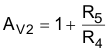
- AV2 is the voltage gain of the second amplifier
where
- f0 is the low-frequency −3 dB corner of the first amplifier
This should be kept well below the audible frequency range.
A design procedure is shown below with an illustrative example using 1% tolerance E96 components for close conformance to the ideal RIAA curve. Because 1% tolerance capacitors are often difficult to find except in 5% or 10% standard values, the design procedure calls for re-calculation of a few component values so that standard capacitor values can be used.
9.2.2.2 RIAA Phono Preamplifier Design Procedure
A design procedure is shown below with an illustrative example using 1% tolerance E96 components for close conformance to the ideal RIAA curve. Since 1% tolerance capacitors are often difficult to find except in 5% or 10% standard values, the design procedure calls for re-calculation of a few component values so that standard capacitor values can be used.
Choose R0. R0 should be small for minimum noise contribution, but not so small that the feedback network excessively loads the amplifier.
Example: Choose R0 = 500
Choose 1 kHz gain, AV1 of first amplifier. This will typically be around 20 dB to 30 dB.
Example: Choose AV1 = 26 dB = 20
Calculate R1 = 8.058 R0AV1
Example: R1 = 8.058 × 500 × 20 = 80.58 k
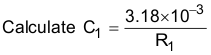
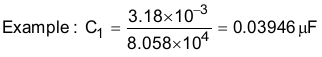
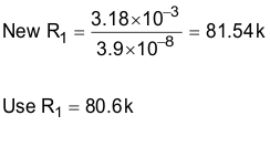
If C1 is not a convenient value, choose the nearest convenient value and calculate a new R1 from Equation 10.
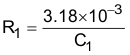
Example: New C1 = 0.039 μF.
Calculate a new value for R0 from Equation 12.
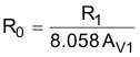
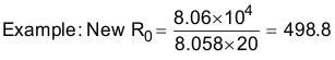
Use R0 = 499.
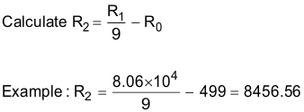
Use R2 = 8.45 K.
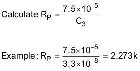
Choose a convenient value for C3 in the range from 0.01 μF to 0.05 μF.
Example: C3 = 0.033 μF
Choose a standard value for R3 that is slightly larger than RP.
Example: R3 = 2.37 k
Calculate R6 from 1 / R6 = 1 / RP − 1 / R3
Example: R6 = 55.36 k
Use 54.9 k
Calculate C4 for low-frequency rolloff below 1 Hz from design Equation 5.
Example: C4 = 2 μF. Use a good quality mylar, polystyrene, or polypropylene.
Choose gain of second amplifier.
Example: The 1 kHz gain up to the input of the second amplifier is about 26 dB for this example. For an overall 1 kHz gain equal to about 36 dB we choose:
AV2 = 10 dB = 3.16
Choose value for R4.
Example: R4 = 2 k
Calculate R5 = (AV2 − 1) R4
Example: R5 = 4.32 k
Use R5 = 4.3 k
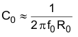
Calculate C0 for low-frequency rolloff below 1 Hz from design Equation 7.
Example: C0 = 200 μF
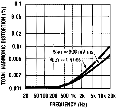
9.2.3 Application Curves for Output Characteristics
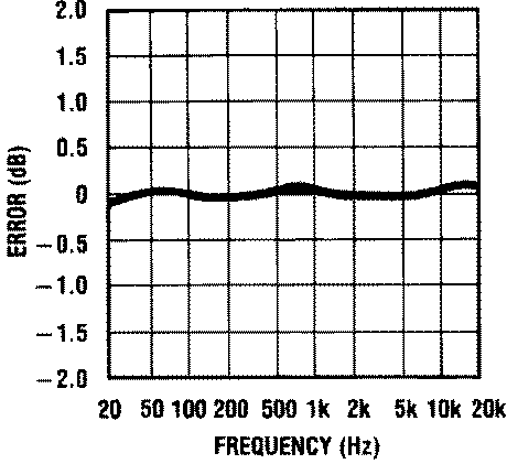
Circuit of Figure 36 Using 1% Resistors
9.3 Typical Application — Reducing Oscillation from High-Capacitive Loads
While all the previously stated operating characteristics are specified with 100-pF load capacitance, the LM833 device can drive higher-capacitance loads. However, as the load capacitance increases, the resulting response pole occurs at lower frequencies, causing ringing, peaking, or oscillation. The value of the load capacitance at which oscillation occurs varies from lot-to-lot. If an application appears to be sensitive to oscillation due to load capacitance, adding a small resistance in series with the load should alleviate the problem (see Figure 39).
9.3.1 Test Schematic
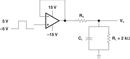 Figure 39. Capacitive Load Testing Circuit
9.3.2 Output Characteristics
Figure 40 through Figure 45 demonstrate the effect adding this small resistance has on the ringing in the output signal.
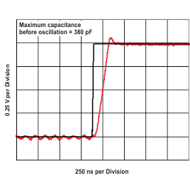 Figure 40. Pulse Response
(RL = 600 Ω, CL = 380 pF)
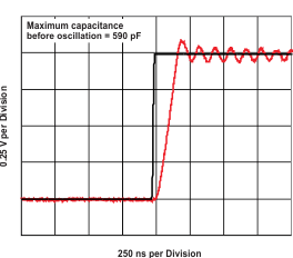 Figure 42. Pulse Response
(RL = 10 kΩ, CL = 590 pF)
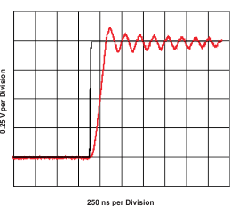 Figure 44. Pulse Response
(RO = 4 Ω, CO = 1000 pF,
RL = 2 kΩ)
 Figure 41. Pulse Response
(RL = 2 kΩ, CL = 560 pF)
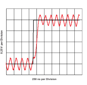 Figure 43. Pulse Response
(RO = 0 Ω, CO = 1000 pF,
RL = 2 kΩ)
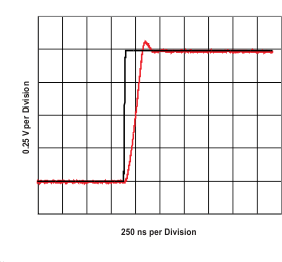 Figure 45. Pulse Response
 (RO = 35 Ω, CO = 1000 pF,
RL = 2 kΩ)