SLOS481B July 2010 – October 2014 LM833
PRODUCTION DATA.
- 1 Features
- 2 Applications
- 3 Description
- 4 Typical Design Example Audio Pre-Amplifier
- 5 Revision History
- 6 Pin Configuration and Functions
- 7 Specifications
- 8 Detailed Description
- 9 Application and Implementation
- 10Power Supply Recommendations
- 11Layout
- 12Device and Documentation Support
- 13Mechanical, Packaging, and Orderable Information
Package Options
Mechanical Data (Package|Pins)
Thermal pad, mechanical data (Package|Pins)
Orderable Information
7 Specifications
7.1 Absolute Maximum Ratings
over operating free-air temperature range (unless otherwise noted)(1)| MIN | MAX | UNIT | |||
|---|---|---|---|---|---|
| VCC+ | Supply voltage(2) | 18 | V | ||
| VCC– | Supply voltage(2) | –18 | V | ||
| VCC+ – VCC– | Supply voltage | 36 | V | ||
| Input voltage, either input(2)(3) | VCC– | VCC+ | V | ||
| Input current(4) | ±10 | mA | |||
| Duration of output short circuit(5) | Unlimited | ||||
| TJ | Operating virtual junction temperature | 150 | °C | ||
(1) Stresses beyond those listed under Absolute Maximum Ratings may cause permanent damage to the device. These are stress ratings only, and functional operation of the device at these or any other conditions beyond those indicated under Recommended Operating Conditions is not implied. Exposure to absolute-maximum-rated conditions for extended periods may affect device reliability.
(2) All voltage values, except differential voltages, are with respect to the midpoint between VCC+ and VCC–.
(3) The magnitude of the input voltage must never exceed the magnitude of the supply voltage.
(4) Excessive input current will flow if a differential input voltage in excess of approximately 0.6 V is applied between the inputs, unless some limiting resistance is used.
(5) The output may be shorted to ground or either power supply. Temperature and/or supply voltages must be limited to ensure the maximum dissipation rating is not exceeded.
7.2 Handling Ratings
| PARAMETER | DEFINITION | MIN | MAX | UNIT |
|---|---|---|---|---|
| Tstg | Storage temperature range | –65 | 150 | °C |
| V(ESD) | Human-Body Model (HBM)(1) | 0 | 2.5 | kV |
| Charged-Device Model (CDM)(2) | 0 | 1.5 |
(1) JEDEC document JEP155 states that 500-V HBM allows safe manufacturing with a standard ESD control process.
(2) JEDEC document JEP157 states that 250-V CDM allows safe manufacturing with a standard ESD control process.
7.3 Recommended Operating Conditions
| MIN | MAX | UNIT | ||
|---|---|---|---|---|
| VCC– | Supply voltage | –5 | –18 | V |
| VCC+ | 5 | 18 | ||
| TA | Operating free-air temperature range | –40 | 85 | °C |
7.4 Thermal Information
| THERMAL METRIC(1) | LM833 | UNIT | ||||
|---|---|---|---|---|---|---|
| D | DGK | P | ||||
| 8 PINS | ||||||
| RθJA | Junction-to-ambient thermal resistance(2)(3) | 97 | 172 | 85 | °C/W | |
(1) For more information about traditional and new thermal metrics, see the IC Package Thermal Metrics application report (SPRA953).
(2) Maximum power dissipation is a function of TJ(max), θJA, and TA. The maximum allowable power dissipation at any allowable ambient temperature is PD = (TJ(max) – TA) / θJA. Operating at the absolute maximum TJ of 150°C can affect reliability.
(3) The package thermal impedance is calculated in accordance with JESD 51-7.
7.5 Electrical Characteristics
VCC– = –15 V, VCC+ = 15 V, TA = 25°C (unless otherwise noted)| PARAMETER | TEST CONDITIONS | MIN | TYP | MAX | UNIT | |||
|---|---|---|---|---|---|---|---|---|
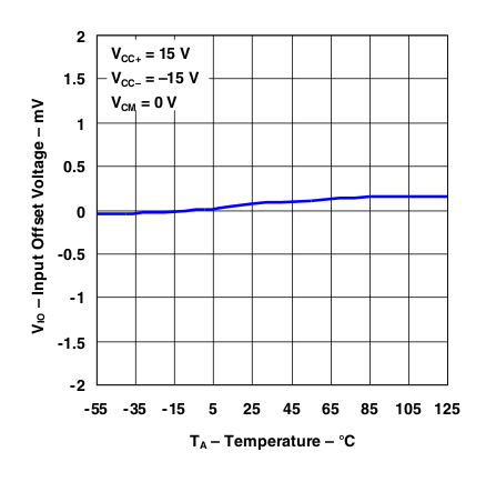
| VIO | Input offset voltage | VO = 0, RS = 10 Ω, VCM = 0 | TA = 25°C | 0.15 | 2 | mV | ||
| TA = –40°C to 85°C | 3 | |||||||
| αVIO | Input offset voltage temperature coefficient | VO = 0, RS = 10 Ω, VCM = 0 | TA = –40°C to 85°C | 2 | μV/°C | |||
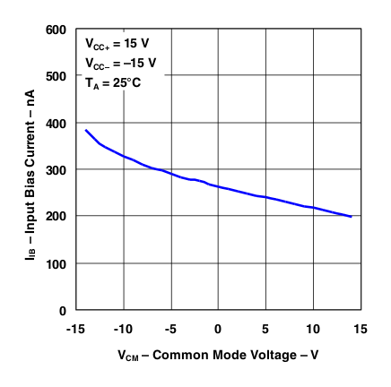
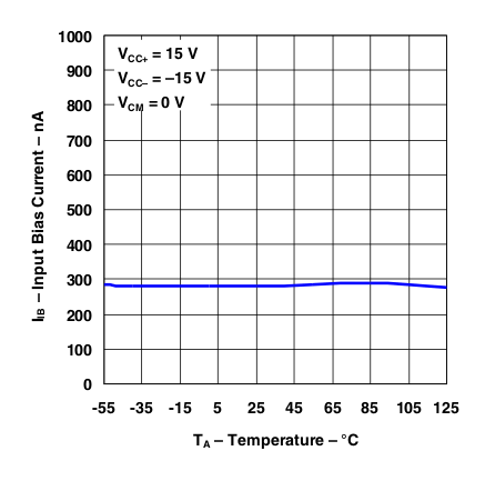
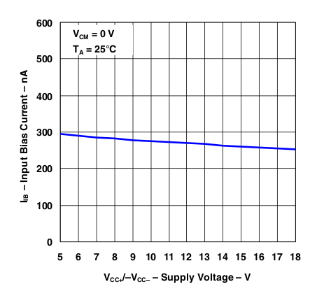
| IIB | Input bias current | VO = 0, VCM = 0 | TA = 25°C | 300 | 750 | nA | ||
| TA = –40°C to 85°C | 800 | |||||||
| IIO | Input offset current | VO = 0, VCM = 0 | TA = 25°C | 25 | 150 | nA | ||
| TA = –40°C to 85°C | 175 | |||||||
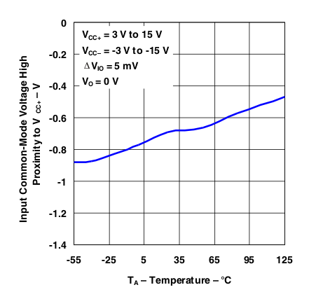
| VICR | Common-mode input voltage range | ΔVIO = 5 mV, VO = 0 | ±13 | ±14 | V | |||
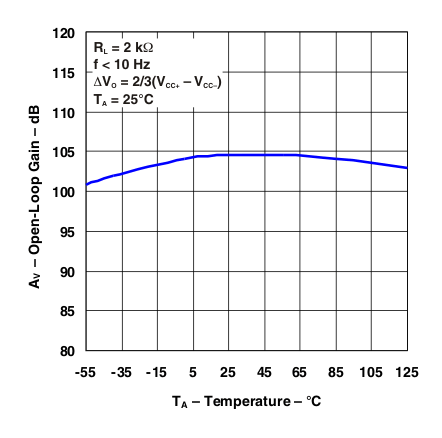
| AVD | Large-signal differential voltage amplification | RL ≥ 2 kΩ, VO = ±10 V | TA = 25°C | 90 | 110 | dB | ||
| TA = –40°C to 85°C | 85 | |||||||
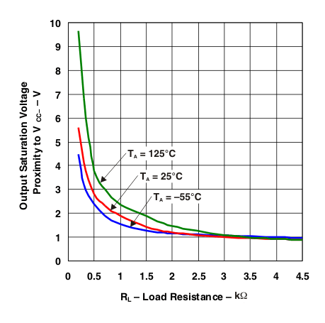
| VOM | Maximum output voltage swing | VID = ±1 V | RL = 600 Ω | VOM+ | 10.7 | V | ||
| VOM– | –11.9 | |||||||
| RL = 2000 Ω | VOM+ | 13.2 | 13.8 | |||||
| VOM– | –13.2 | –13.7 | ||||||
| RL = 10,000 Ω | VOM+ | 13.5 | 14.1 | |||||
| VOM– | –14 | –14.6 | ||||||
| CMMR | Common-mode rejection ratio | VIN = ±13 V | 80 | 100 | dB | |||
| kSVR(1) | Supply-voltage rejection ratio | VCC+ = 5 V to 15 V, VCC– = –5 V to –15 V | 80 | 105 | dB | |||
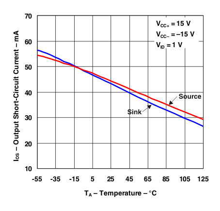
| IOS | Output short-circuit current | |VID| = 1 V, Output to GND | Source current | 15 | 29 | mA | ||
| Sink current | –20 | –37 | ||||||
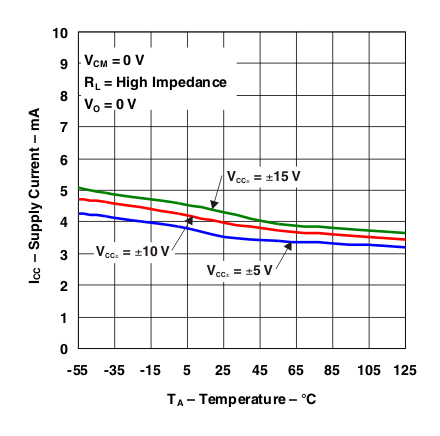
| ICC | Supply current (per channel) | VO = 0 | TA = 25°C | 2.05 | 2.5 | mA | ||
| TA = –40°C to 85°C | 2.75 | |||||||
(1) Measured with VCC± differentially varied at the same time
7.6 Operating Characteristics
VCC– = –15 V, VCC+ = 15 V, TA = 25°C (unless otherwise noted)| PARAMETER | TEST CONDITIONS | MIN | TYP | MAX | UNIT | ||
|---|---|---|---|---|---|---|---|
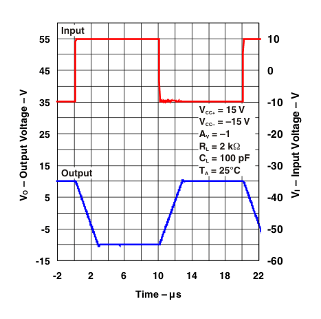
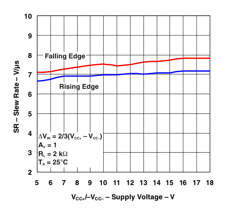
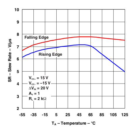
| SR | Slew rate at unity gain | AVD = 1, VIN = –10 V to 10 V, RL = 2 kΩ, CL = 100 pF | 5 | 7 | V/μs | ||
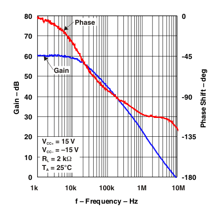
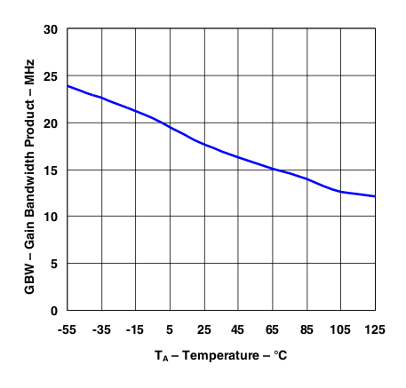
| GBW | Gain bandwidth product | f = 100 kHz | 10 | 16 | MHz | ||
| B1 | Unity gain frequency | Open loop | 9 | MHz | |||
| Gm | Gain margin | RL = 2 kΩ | CL = 0 pF | –11 | dB | ||
| CL = 100 pF | –6 | ||||||
| Φm | Phase margin | RL = 2 kΩ | CL = 0 pF | 55 | degrees | ||
| CL = 100 pF | 40 | ||||||
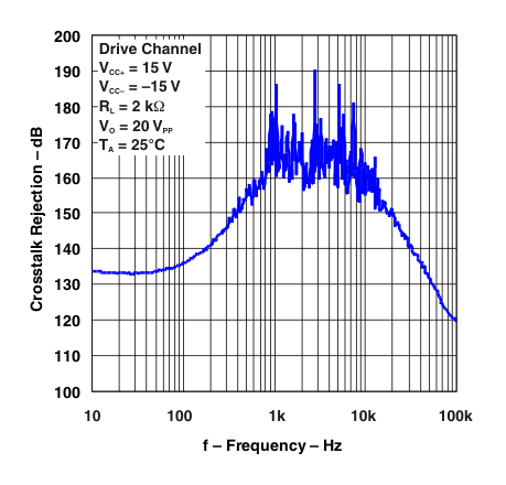
| Amp-to-amp isolation | f = 20 Hz to 20 kHz | –120 | dB | ||||
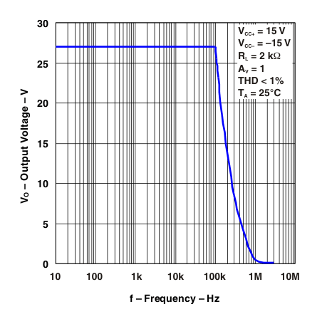
| Power bandwidth | VO = 27 V(PP), RL = 2 kΩ, THD ≤ 1% | 120 | kHz | ||||
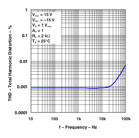
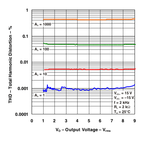
| THD | Total harmonic distortion | VO = 3 Vrms, AVD = 1, RL = 2 kΩ, f = 20 Hz to 20 kHz | 0.002% | ||||
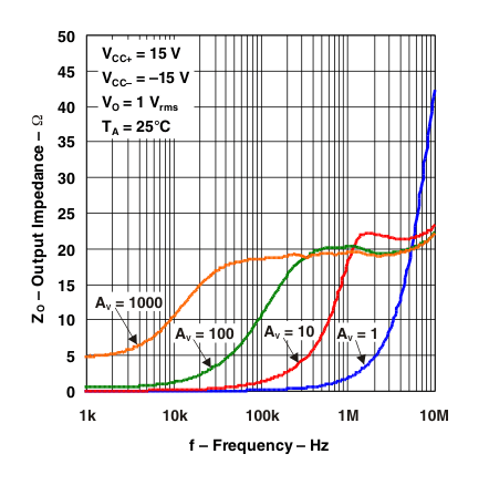
| zo | Open-loop output impedance | VO = 0, f = 9 MHz | 37 | Ω | |||
| rid | Differential input resistance | VCM = 0 | 175 | kΩ | |||
| Cid | Differential input capacitance | VCM = 0 | 12 | pF | |||
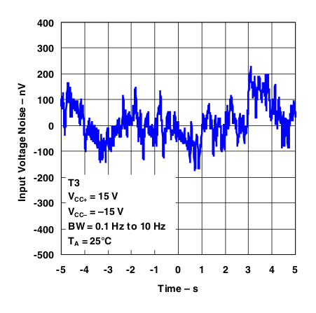
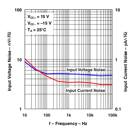
| Vn | Equivalent input noise voltage | f = 1 kHz, RS = 100 Ω | 4.5 | nV/√Hz | |||
| In | Equivalent input noise current | f = 1 kHz | 0.5 | pA/√Hz | |||
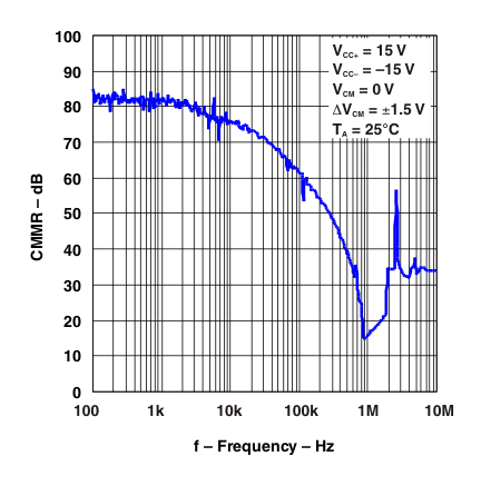
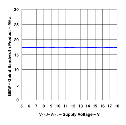
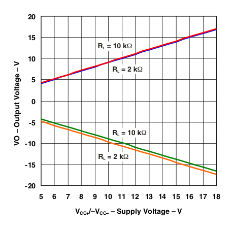
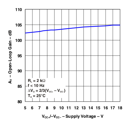
7.7 Typical Characteristics
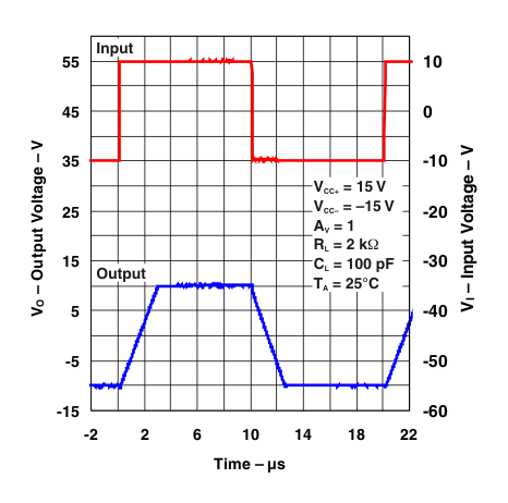
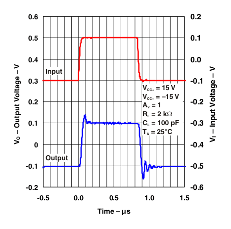
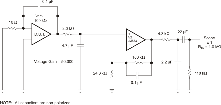 Figure 1. Voltage Noise Test Circuit (0.1 Hz to 10 Hz)
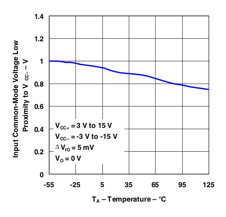
to VCC– vs Temperature
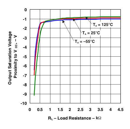
vs Load Resistance
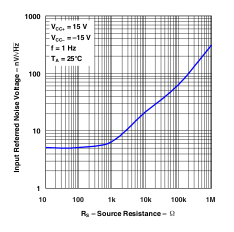
vs Source Resistance
to VCC+ vs Temperature
vs Load Resistance

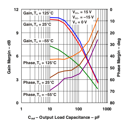
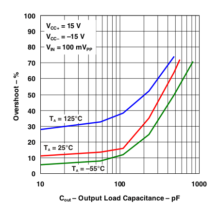
vs Output Load Capacitance
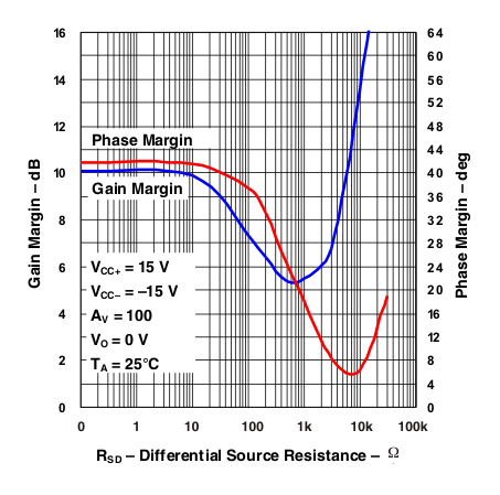
vs Differential Source Resistance