SNIS139F February 2005 – January 2024 LM95231
PRODUCTION DATA
- 1
- 1 Features
- 2 Applications
- 3 Description
- 4 Pin Configuration and Functions
- 5 Specifications
- 6 Detailed Description
-
7 Registers
- 7.1 LM95231 Registers
- 7.2 Status Register
- 7.3 Configuration Register
- 7.4 Remote Diode Filter Control Register
- 7.5 Remote Diode Model Type Select Register
- 7.6 Remote TruTherm Mode Control
- 7.7 Local and Remote MSB and LSB Temperature Registers
- 7.8 Manufacturers ID Register
- 7.9 Die Revision Code Register
- 8 Application and Implementation
- 9 Layout
- 10Device and Documentation Support
- 11Revision History
- 12Mechanical, Packaging, and Orderable Information
Package Options
Mechanical Data (Package|Pins)
- DGK|8
Thermal pad, mechanical data (Package|Pins)
Orderable Information
6.3.7 Communicating with the LM95231
The data registers in the LM95231 are selected by the Command Register. At power-up the Command Register is set to “00”, the location for the Read Local Temperature Register. The Command Register latches the last location it was set to. Each data register in the LM95231 falls into one of four types of user accessibility:
- Read only
- Write only
- Write/Read same address
- Write/Read different address
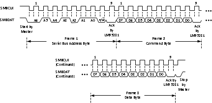
A Write to the LM95231 will always include the address byte and the command byte. A write to any register requires one data byte.
Reading the LM95231 can take place either of two ways:
- If the location latched in the Command Register is correct (most of the time it is expected that the Command Register will point to one of the Read Temperature Registers because that will be the data most frequently read from the LM95231), then the read can simply consist of an address byte, followed by retrieving the data byte.
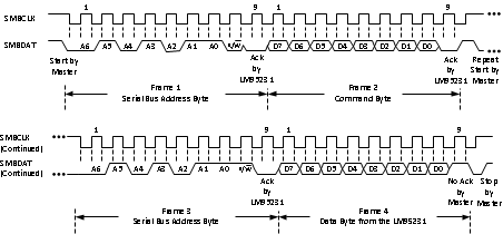
- If the Command Register needs to be set, then an address byte, command byte, repeat start, and another address byte will accomplish a read.
The data byte has the most significant bit first. At the end of a read, the LM95231 can accept either acknowledge or No Acknowledge from the Master (No Acknowledge is typically used as a signal for the slave that the Master has read its last byte). When retrieving all 11 bits from a previous remote diode temperature measurement, the master must insure that all 11 bits are from the same temperature conversion. This may be achieved by reading the MSB register first. The LSB will be locked after the MSB is read. The LSB will be unlocked after being read. If the user reads MSBs consecutively, each time the MSB is read, the LSB associated with that temperature will be locked in and override the previous LSB value locked-in.
 Figure 6-2 Serial Bus Write to the
Internal Command Register
 Figure 6-3 Serial Bus Write to the internal Command Register followed by a Data Byte
 Figure 6-4 Serial Bus byte Read from a Register with the internal Command Register preset to desired value.