SNAS425C October   2007  – October 2014 LM98519

PRODUCTION DATA.  

  1. Features
  2. Applications
  3. Description
  4. Revision History
  5. Pin Configuration and Functions
  6. Specifications
    1. 6.1 Absolute Maximum Ratings
    2. 6.2 Handling Ratings
    3. 6.3 Recommended Operating Conditions
    4. 6.4 Thermal Information
    5. 6.5 Electrical Characteristics
    6. 6.6 Serial Interface Timing
  7. Detailed Description
    1. 7.1 Overview
    2. 7.2 Functional Block Diagrams
    3. 7.3 Feature Description
      1. 7.3.1 Input Clamping and Biasing Circuitry
      2. 7.3.2 Input Connections for 3 Channel Operation
      3. 7.3.3 AFE References
      4. 7.3.4 Offset Control
      5. 7.3.5 Black Level Calibration (Offset)
        1. 7.3.5.1 Manual Offset Adjustment
        2. 7.3.5.2 Automatic Offset Adjustment
        3. 7.3.5.3 Gain Control
        4. 7.3.5.4 White Level Calibration (AGC - Automatic Gain Control)
      6. 7.3.6 Operating Mode Description
    4. 7.4 Device Functional Modes
      1. 7.4.1 AFEPHASEn Details for SHP/SHD Input Mode
      2. 7.4.2 AFEPHASEn Details for SAMPLE and HOLD Input Mode
      3. 7.4.3 AFEPHASEn: 6 Channel and 3 Channel Modes
      4. 7.4.4 LM98519 AFEPHASE Synchronization
      5. 7.4.5 Sampling Timing Diagrams
    5. 7.5 Programming
      1. 7.5.1  Using Black Pixel Average
      2. 7.5.2  Sample Timing Control
      3. 7.5.3  Timing Monitor Outputs
      4. 7.5.4  Output Data Test Pattern Generation
      5. 7.5.5  Fixed Pattern
      6. 7.5.6  Horizontal Gradation
      7. 7.5.7  Vertical Gradation
      8. 7.5.8  Lattice Pattern
      9. 7.5.9  Serial Interface
      10. 7.5.10 Serial Write
      11. 7.5.11 Serial Read
    6. 7.6 Register Maps
      1. 7.6.1 Configuration Registers
      2. 7.6.2 Configuration Register Details
  8. Application and Implementation
    1. 8.1 Design Requirements
    2. 8.2 Detailed Design Procedure
  9. Power Supply Recommendations
    1. 9.1 Over Voltage Protection on OS Inputs
  10. 10Layout
    1. 10.1 Layout Guidelines
    2. 10.2 Layout Example
  11. 11Device and Documentation Support
    1. 11.1 Documentation Support
      1. 11.1.1 Related Documentation
    2. 11.2 Trademarks
    3. 11.3 Electrostatic Discharge Caution
    4. 11.4 Glossary
  12. 12Mechanical, Packaging, and Orderable Information

Package Options

Mechanical Data (Package|Pins)
Thermal pad, mechanical data (Package|Pins)
Orderable Information

10 Layout

10.1 Layout Guidelines

  1. Use Figure 35 configuration for powering the device.
  2. static_voltage_example.gif
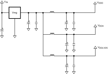
Figure 35. Recommended Setup for Powering Device
  3. Place decoupling cap(s) next to every supply pin to the ground plane close by.
  4. Use a multi-layer boards as shown in Figure 35 to ease routing, and to provide a low inductance ground plane.
  5. Beware of via inductance and when necessary increase the number and / or diameter of vias to reduce inductance
  6. Use ground plane “keep out” areas under sensitive nodes to minimize parasitic capacitance

10.2 Layout Example

layout_guideline.gif
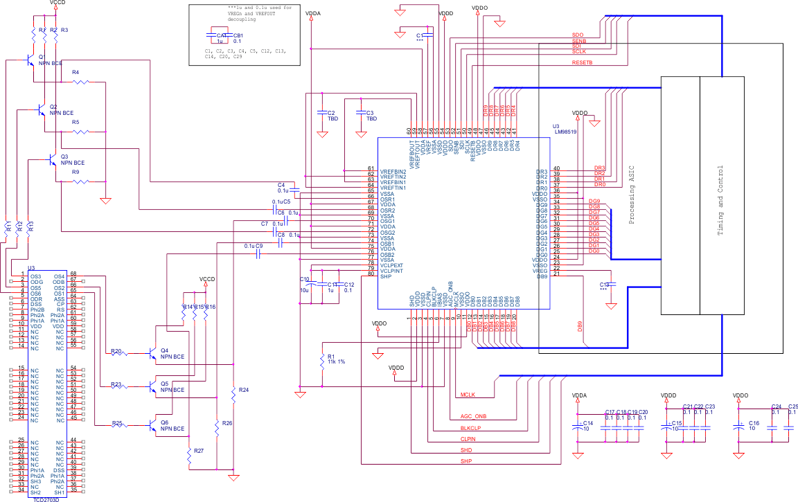
Figure 36. LM98519 Typical Application