SNOSBY1C June 1999 – December 2015 LMC567
PRODUCTION DATA.
- 1 Features
- 2 Applications
- 3 Description
- 4 Revision History
- 5 Device Comparison Table
- 6 Pin Configuration and Functions
- 7 Specifications
- 8 Parameter Measurement Information
- 9 Detailed Description
- 10Application and Implementation
- 11Power Supply Recommendations
- 12Layout
- 13Device and Documentation Support
- 14Mechanical, Packaging, and Orderable Information
Package Options
Mechanical Data (Package|Pins)
- D|8
Thermal pad, mechanical data (Package|Pins)
Orderable Information
1 Features
- Functionally Similar to LM567
- 2-V to 9-V Supply Voltage Range
- Low Supply Current Drain
- No Increase in Current With Output Activated
- Operates to 500-kHz Input Frequency
- High Oscillator Stability
- Ground-Referenced Input
- Hysteresis Added to Amplitude Comparator
- Out-of-Band Signals and Noise Rejected
- 20-mA Output Current Capability
2 Applications
- Touch-Tone Decoding
- Precision Oscillators
- Frequency Monitoring and Control
- Wide-Band FSK Demodulation
- Ultrasonic Controls
- Carrier Current Remote Controls
- Communications Paging Decoders
3 Description
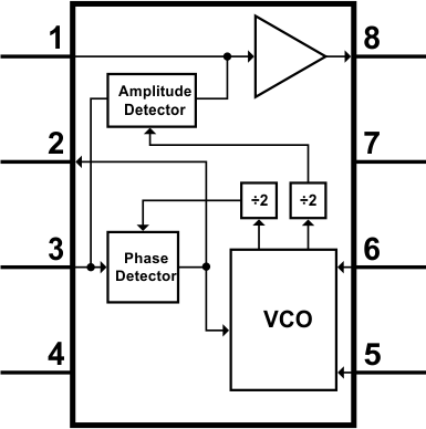
The LMC567 device is a low-power, general-purpose LMCMOS tone decoder which is functionally similar to the industry standard LM567. The device consists of a twice frequency voltage-controlled oscillator (VCO) and quadrature dividers which establish the reference signals for phase and amplitude detectors.
The phase detector and VCO form a phase-locked loop (PLL) which locks to an input signal frequency which is within the control range of the VCO. When the PLL is locked and the input signal amplitude exceeds an internally pre-set threshold, a switch to ground is activated on the output pin. External components set up the oscillator to run at twice the input frequency and determine the phase and amplitude filter time constants.
Device Information (1)
| PART NUMBER | PACKAGE | BODY SIZE (NOM) |
|---|---|---|
| LMC567 | SOIC (8) | 4.90 mm × 3.91 mm |
- For all available packages, see the orderable addendum at the end of the data sheet.
Simplified Diagram
