SNOSBY1C June 1999 – December 2015 LMC567
PRODUCTION DATA.
- 1 Features
- 2 Applications
- 3 Description
- 4 Revision History
- 5 Device Comparison Table
- 6 Pin Configuration and Functions
- 7 Specifications
- 8 Parameter Measurement Information
- 9 Detailed Description
- 10Application and Implementation
- 11Power Supply Recommendations
- 12Layout
- 13Device and Documentation Support
- 14Mechanical, Packaging, and Orderable Information
Package Options
Mechanical Data (Package|Pins)
- D|8
Thermal pad, mechanical data (Package|Pins)
Orderable Information
10 Application and Implementation
NOTE
Information in the following applications sections is not part of the TI component specification, and TI does not warrant its accuracy or completeness. TI’s customers are responsible for determining suitability of components for their purposes. Customers should validate and test their design implementation to confirm system functionality.
10.1 Application Information
These typical connection diagrams highlight the required external components and system level connections for proper operation of the device in several popular use cases.
Any design variation can be supported by TI through schematic and layout reviews. Visit support.ti.com for additional design assistance. Also, join the audio amplifier discussion forum at e2e.ti.com.
10.2 Typical Application
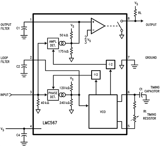
 Figure 8. LMC567 Application Schematic
10.2.1 Design Requirements
For this design example, use the parameters listed in Table 2.
Table 2. Design Parameters
| DESIGN PARAMETER | EXAMPLE VALUE |
|---|---|
| Supply voltage | 2 V to 9 V |
| Input voltage | 20 mVRMS to (VCC + 0.5) |
| Input frequency | 1 Hz to 500 KHz |
| Output current maximum | 30 mA |
10.2.2 Detailed Design Procedure
10.2.2.1 Timing Components
As VCO frequency (FOSC) runs at twice the frequency of the input tone, the desired input detection frequency can be defined by Equation 7:

The central frequency of the oscillator is set by timing capacitor and resistor. The timing capacitor value (CT) must be set in order to calculate the timing resistor value (RT). This is given by Equation 8:

So, in order to found the required component values to set the detection frequency Equation 9:

This approximation is valid with lower frequencies; considerations must be taken when using higher frequencies. More information on this can be found in Oscillator.
10.2.2.2 Bandwidth
Detection bandwidth is represented as a percentage of FOSC. It can be approximated as a function of FOSC × C2 following the behavior indicated in Figure 4. More information on this can be found in Loop Filter.
10.2.2.3 Output Filter
The size of the output filter capacitor C1 is a tradeoff between slew rate and carrier ripple. More information on this can be found in Output Filter.
10.2.2.4 Supply Decoupling
The decoupling of supply pin 4 becomes more critical at high supply voltages with high operating frequencies, requiring C4 to be placed as close as possible to pin 4.
10.2.3 Application Curve
SPACE
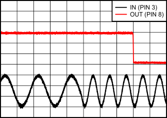
 Figure 9. Frequency Detection