SNOSD61 June 2017 LMC6482-MIL
PRODUCTION DATA.
- 1 Features
- 2 Applications
- 3 Description
- 4 Pin Configuration and Functions
- 5 Specifications
- 6 Detailed Description
- 7 Application and Implementation
- 8 Power Supply Recommendations
- 9 Layout
- 10Device and Documentation Support
- 11Mechanical, Packaging, and Orderable Information
Package Options
Mechanical Data (Package|Pins)
- Y|0
Thermal pad, mechanical data (Package|Pins)
Orderable Information
1 Features
- Typical Unless Otherwise Noted
- Rail-to-Rail Input Common-Mode Voltage Range (Ensured Over Temperature)
- Rail-to-Rail Output Swing (Within 20-mV of Supply Rail, 100-kΩ Load)
- Ensured 3-V, 5-V, and 15-V Performance
- Excellent CMRR and PSRR: 82 dB
- Ultralow Input Current: 20 fA
- High Voltage Gain (R L = 500 k Ω): 130 dB
- Specified for 2-kΩ and 600-Ω Loads
- Power-Good Output
- Available in VSSOP Package
2 Applications
- Data Acquisition Systems
- Transducer Amplifiers
- Hand-held Analytic Instruments
- Medical Instrumentation
- Active Filter, Peak Detector, Sample and Hold, pH Meter, Current Source
- Improved Replacement for TLC272, TLC277
3 Description
The LMC6482-MIL device provides a common-mode range that extends to both supply rails. This rail-to-rail performance combined with excellent accuracy, due to a high CMRR, makes it unique among rail-to-rail input amplifiers. The device is ideal for systems, such as data acquisition, that require a large input signal range. The LMC6482-MIL is also an excellent upgrade for circuits using limited common-mode range amplifiers such as the TLC272 and TLC277.
Maximum dynamic signal range is assured in low voltage and single supply systems by the rail-to-rail output swing of the LMC6482-MIL. The rail-to-rail output swing is ensured for loads down to 600 Ω of the device. Ensured low-voltage characteristics and low-power dissipation make the LMC6482-MIL especially well-suited for battery-operated systems. LMC6482-MIL is also available in a VSSOP package, which is almost half the size of a SOIC-8 device. See the LMC6484 data sheet for a quad CMOS operational amplifier with these same features.
Device Information(1)
| PART NUMBER | PACKAGE | BODY SIZE (NOM) |
|---|---|---|
| LMC6482-MIL | SOIC (8) | 4.90 mm × 3.91 mm |
| VSSOP (8) | 3.00 mm × 3.00 mm | |
| PDIP (8) | 9.81 mm × 6.35 mm |
- For all available packages, see the orderable addendum at the end of the data sheet.
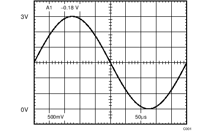
Rail-to-Rail Input

Rail-to-Rail Output
