SNOSD61 June   2017 LMC6482-MIL

PRODUCTION DATA.  

  1. Features
  2. Applications
  3. Description
  4. Pin Configuration and Functions
  5. Specifications
    1. 5.1 Absolute Maximum Ratings
    2. 5.2 ESD Ratings
    3. 5.3 Recommended Operating Conditions
    4. 5.4 Thermal Information
    5. 5.5 Electrical Characteristics for V+ = 5 V
    6. 5.6 Electrical Characteristics for V+ = 3 V
    7. 5.7 Typical Characteristics
  6. Detailed Description
    1. 6.1 Overview
    2. 6.2 Functional Block Diagram
    3. 6.3 Feature Description
      1. 6.3.1 Amplifier Topology
      2. 6.3.2 Input Common-Mode Voltage Range
      3. 6.3.3 Rail-to-Rail Output
    4. 6.4 Device Functional Modes
  7. Application and Implementation
    1. 7.1 Application Information
      1. 7.1.1 Upgrading Applications
      2. 7.1.2 Data Acquisition Systems
      3. 7.1.3 Instrumentation Circuits
      4. 7.1.4 Spice Macromodel
    2. 7.2 Typical Applications
      1. 7.2.1 3-V Single Supply Buffer Circuit
        1. 7.2.1.1 Design Requirements
        2. 7.2.1.2 Detailed Design Procedure
          1. 7.2.1.2.1 Capacitive Load Compensation
            1. 7.2.1.2.1.1 Capacitive Load Tolerance
            2. 7.2.1.2.1.2 Compensating for Input Capacitance
            3. 7.2.1.2.1.3 Offset Voltage Adjustment
        3. 7.2.1.3 Application Curves
      2. 7.2.2 Typical Single-Supply Applications
  8. Power Supply Recommendations
  9. Layout
    1. 9.1 Layout Guidelines
    2. 9.2 Layout Example
  10. 10Device and Documentation Support
    1. 10.1 Trademarks
    2. 10.2 Electrostatic Discharge Caution
    3. 10.3 Glossary
  11. 11Mechanical, Packaging, and Orderable Information

Package Options

Mechanical Data (Package|Pins)
  • Y|0
Thermal pad, mechanical data (Package|Pins)
Orderable Information

Pin Configuration and Functions

D, DGK and P Packages
8-Pin SOIC, VSSOP and PDIP
(Top View)
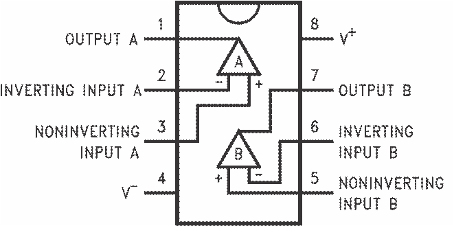
LMC6482-MIL 01171304.png

Pin Functions

PIN TYPE DESCRIPTION
NO. NAME
1 OUTPUT A O Output for Amplifier A
2 INVERTING INPUT A I Inverting input for Amplifier A
3 NONINVERTING INPUT A I Noninverting input for Amplifier A
4 V P Negative supply voltage input
5 NONINVERTING INPUT B I Noninverting input for Amplifier B
6 INVERTING INPUT B I Inverting input for Amplifier B
7 OUTPUT B O Output for Amplifier B
8 V+ P Positive supply voltage input