SNLS247H April 2007 – June 2016 LMH0302
PRODUCTION DATA.
- 1 Features
- 2 Applications
- 3 Description
- 4 Revision History
- 5 Pin Configuration and Functions
- 6 Specifications
- 7 Detailed Description
- 8 Application and Implementation
- 9 Power Supply Recommendations
- 10Layout
- 11Device and Documentation Support
- 12Mechanical, Packaging, and Orderable Information
Package Options
Mechanical Data (Package|Pins)
- RUM|16
Thermal pad, mechanical data (Package|Pins)
- RUM|16
Orderable Information
8 Application and Implementation
NOTE
Information in the following applications sections is not part of the TI component specification, and TI does not warrant its accuracy or completeness. TI’s customers are responsible for determining suitability of components for their purposes. Customers should validate and test their design implementation to confirm system functionality.
8.1 Application Information
The LMH0302 is a single-channel SDI cable driver that supports different application spaces. The following sections describe the typical use cases and common implementation practices.
8.1.1 General Guidance for All Applications
The SMPTE specifications define the use of AC-coupling capacitors for transporting uncompressed serial data streams with heavy low-frequency content. This specification requires the use of a 4.7-µF AC-coupling capacitor to avoid low frequency DC wander. The 75-Ω signal is also required to meet certain rise and fall timing to facilitate highest eye opening for the receiving device.
SMPTE specifies the requirements for the Serial Digital Interface to transport digital video at SD, HD, 3 Gbps, and higher data rates over coaxial cables. One of the requirements is meeting the required return loss. This requirement specifies how closely the port resembles 75-Ω impedance across a specified frequency band. Output return loss is dependent on board design. The LMH0302 supports these requirements.
8.2 Typical Application
 Figure 3. Application Circuit
8.2.1 Design Requirements
For the LMH0302 design example, Table 1 lists the design parameters.
Table 1. LMH0302 Design Parameters
| PARAMETER | REQUIREMENT |
|---|---|
| Input termination | Required; 49.9 Ω are recommended (see Figure 3). |
| Output AC-coupling capacitors | Required; both SDO and SDO require AC-coupling capacitors. SDO AC-coupling capacitors are expected to be 4.7 µF to comply with SMPTE wander requirement. |
| DC power supply coupling capacitors | To minimize power supply noise, place 0.1-µF capacitor as close to the device VCC pin as possible. |
| Distance from device to BNC | Keep this distance as short as possible. |
| High speed SDI and SDI trace impedance | Design differential trace impedance of SDI and SDI with 100 Ω. |
| High speed SDO and SDO trace impedance | Single-ended trace impedance for SDO and SDO with 75 Ω. |
8.2.2 Detailed Design Procedure
The following design procedure is recommended:
- Select a suitable power supply voltage for the LMH0302. It can be powered from a single 3.3-V supply.
- Check that the power supply meets the DC requirements in Electrical Characteristics – DC.
- Select the proper pull-high or pull-low for SD/HD to set the slew rate.
- Select proper pull-high or pull-low for ENABLE to enable or disable the output driver.
- Choose a high-quality 75-Ω BNC that is capable to support 2.97-Gbps applications. Consult a BNC supplier regarding insertion loss, impedance specifications, and recommended BNC footprint for meeting SMPTE return loss requirements.
- Choose small 0402 surface-mount ceramic capacitors for the AC-coupling and bypass capacitors.
- Use proper footprint for BNC and AC-coupling capacitors. Anti-pads are commonly used in power and ground planes under these landing pads to achieve optimum return loss.
8.2.3 Application Curves
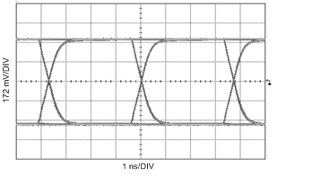
 Figure 4. SDO PRBS10 at 270 Mbps
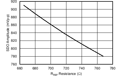
 Figure 5. SDO Amplitude vs RREF Resistance