SNLS285H April 2008 – May 2016 LMH0303
PRODUCTION DATA.
- 1 Features
- 2 Applications
- 3 Description
- 4 Revision History
- 5 Pin Configuration and Functions
- 6 Specifications
- 7 Detailed Description
- 8 Application and Implementation
- 9 Power Supply Recommendations
- 10Layout
- 11Device and Documentation Support
- 12Mechanical, Packaging, and Orderable Information
Package Options
Mechanical Data (Package|Pins)
- RUM|16
Thermal pad, mechanical data (Package|Pins)
- RUM|16
Orderable Information
7 Detailed Description
7.1 Overview
The LMH0303 ST 424, ST292, ST259 serial digital cable driver is a monolithic, high-speed cable driver designed for use in serial digital video data transmission applications. The LMH0303 drives 75-Ω transmission lines (Belden 8281, 1694A, Canare L-5CFB, or equivalent) at data rates up to 2.97 Gbps.
The LMH0303 provides two selectable slew rates for ST 259 and ST 292/424 compliance. The output voltage swing is adjustable through a single external resistor ( RREF) or SMBus interface in 5-mV steps.
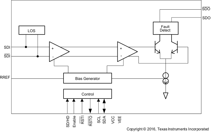
The LMH0303 cable detect feature senses near-end termination to determine if a cable is attached to the output BNC. The LMH0303 input loss of signal (LOS) detects the presence of a valid signal at the 100-Ω differential input of the cable driver. These features can be used to activate power-save mode. These features are accessible through an SMBus interface.
The LMH0303 is powered from a single 3.3 V supply. Power consumption is typically 130 mW in SD mode and 155 mW in HD mode. The LMH0303 is available in a 16-pin WQFN package.
7.2 Functional Block Diagram

7.3 Feature Description
The LMH0303 data path consists of several key blocks as shown in the Functional Block Diagram. These key circuits are:
- Loss-of-signal detector
- Input interfacing
- Output interfacing
- Output slew rate control
- Cable fault detection
- SMBus configuration
7.3.1 Loss-of-Signal Detector
The LMH0303 detects when the input signal does not have a video-like pattern. Self-oscillation and low levels of noise are rejected. This loss-of-signal detector allows a very sensitive input stage that is robust against coupled noise without any degradation of jitter performance. Through the SMBus, the loss-of-signal detector can either add an input offset or mute the outputs. An offset is added by default. Additionally, the loss-of-signal detector can be linked to the ENABLE functionality so that when the LOS goes low, ENABLE also goes low.
7.3.2 Input Interfacing
The LMH0303 accepts either differential or single-ended input. For single-ended operation, the unused input must be properly terminated.
7.3.3 Output Interfacing
The LMH0303 uses current mode outputs. Single-ended output levels are 800 mVP-P into 75-Ω AC-coupled coaxial cable with an RREF resistor value of 750 Ω. The RREF resistor is connected between the RREF pin and VCC.
The RREF resistor should be placed as close as possible to the RREF pin. In addition, the copper in the plane layers below the RREF network should be removed to minimize parasitic capacitance.
7.3.4 Output Slew Rate Control
The LMH0303 output rise and fall times are selectable for either ST259 or ST 424 or 292 compliance through the SD/HD pin. For slower rise and fall times, or ST 259 compliance, SD/HD is set high. For faster rise and fall times, or ST 424 and ST 292 compliance, SD/HD is set low. SD/HD may also be controlled using the SMBus, provided the SD/HD pin is held low. SD/HD has an internal pulldown.
7.3.5 Cable Fault Detection
The LMH0303 termination fault detection purpose is to provide an indication when no cable is connected to the output (near end). The termination fault detection works by detecting reflections on the output. The device measures the peak-to-peak output voltage. The output amplitude is normally 800 mVp-p. No termination results in 2x the output voltage (1600 mVp-p) due to the 100% reflection.
When a video signal (or AC test signal) is present on SDI, the device senses the SDO and SDO amplitudes. If the output is not properly terminated (through a terminated cable or local termination), the amplitude will be higher than expected, and the termination fault signal is asserted. The termination fault signal is deasserted when the proper termination is applied. This feature allows the system designer the flexibility to react to cable attachment and removal. Note that a long length of cable will look like a proper termination at the device output. The cable driver must be enabled for the termination detection to operate. If the termination fault will be used to power down the LMH0303, then periodic polling (enabling) is recommended to monitor the output termination. For example, when a fault condition is triggered, ENABLE can be driven low to power down the device. The LMH0303 should be re-enabled periodically to check the status of the output termination. The LMH0303 must be powered on for at least 4 ms for termination fault detection to work.
7.3.6 SMBus Interface
The System Management Bus (SMBus) is a two-wire interface designed for the communication between various system component chips. By accessing the control functions of the circuit through the SMBus, pin count is kept to a minimum while allowing a maximum amount of versatility. The LMH0303 has several internal configuration registers which may be accessed through the SMBus.
The 7-bit default address for the LMH0303 is 0x17. The LSB is set to 0'b for a WRITE and 1'b for a READ, so the 8-bit default address for a WRITE is 0x2E and the 8-bit default address for a READ is 0x2F. The SMBus address may be dynamically changed.
In applications where there might be several LMH0303s, the SDA, SCL, and FAULT pins can be shared. The SCL, SDA, and FAULT pins are open drain and require external pullup resistors. Multiple LMH0303s may have the FAULT pin wire ORed. This signal becomes active when either loss of signal is detected or any termination faults are detected. The registers may be read in order to determine the cause. Additionally, each signal can be masked from the FAULT pin.
7.3.6.1 Transfer of Data through the SMBus
During normal operation the data on SDA must be stable during the time when SCL is High.
There are three unique states for the SMBus:
START: A High-to-Low transition on SDA while SCL is High indicates a message START condition.
STOP: A Low-to-High transition on SDA while SCL is High indicates a message STOP condition.
IDLE: If SCL and SDA are both High for a time exceeding tBUF from the last detected STOP condition or if they are High for a total exceeding the maximum specification for tHIGH, then the bus will transfer to the IDLE state.
7.3.6.2 SMBus Transactions
The device supports WRITE and READ transactions. See Table 1 for register address, type (Read/Write, Read Only), default value, and function information.
7.3.6.2.1 Writing a Register
To write a register, the following protocol is used (see SMBus 2.0 specification).
- The Host drives a START condition, the 7-bit SMBus address, and a 0 indicating a WRITE.
- The Device (Slave) drives the ACK bit (0).
- The Host drives the 8-bit Register Address.
- The Device drives an ACK bit (0).
- The Host drives the 8-bit data byte.
- The Device drives an ACK bit (0).
- The Host drives a STOP condition.
The WRITE transaction is completed, the bus goes IDLE, and communication with other SMBus devices may now occur.
7.3.6.2.2 Reading a Register
To read a register, the following protocol is used (see SMBus 2.0 specification).
- The Host drives a START condition, the 7-bit SMBus address, and a 0 indicating a WRITE.
- The Device (Slave) drives the ACK bit (0).
- The Host drives the 8-bit Register Address.
- The Device drives an ACK bit (0).
- The Host drives a START condition.
- The Host drives the 7-bit SMBus Address, and a 1 indicating a READ.
- The Device drives an ACK bit 0.
- The Device drives the 8-bit data value (register contents).
- The Host drives a NACK bit 1 indicating end of the READ transfer.
- The Host drives a STOP condition.
7.3.6.3 Communicating With Multiple LMH0303 Cable Drivers through the SMBus
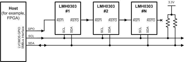
A common application for the LMH0303 uses multiple cable driver devices. Even though the LMH0303 devices all have the same default SMBus device ID (address), it is still possible for them share the SMBus signals as shown in Figure 4. A third signal is required from the host to the first device. This signal acts as a Enable or Reset signal. Additional LMH0303s are controlled from the upstream device. In this control scheme, multiple LMH0303s may be controlled through the two-wire SMBus and the use of one General Purpose Output (GPO) signal. Other SMBus devices may also be connected to the two wires, assuming they have their own unique SMBus addresses.
 Figure 4. SMBus Configuration for Multiple LMH0303 Cable Drivers
The RSTI pin of the first device is controlled by the system with a GPO pin from the host. The first LMH0303 RSTO pin is then daisy chained to the next device's RSTI pin. That device’s RSTO pin is connected to the next device and so on.
The procedure at initialization is to:
- Hold the host GPO pin Low in RESET, to the first device. RSTO output default is also Low which holds the next device in RESET in the chain.
- Raise the host GPO signal to LMH0303 #1 RSTI input pin.
- Write to Address 0x2E Register 0 with the new address value (for example 0x2C).
- Upon writing Register 0 in LMH0303 #1, its RSTO signal will switch High. Its new address is 0x2C, and the next LMH0303 in the chain will now respond to the default address of 0x2E.
- The process is repeated until all LMH0303 devices have a unique address loaded.
- Direct SMBus writes and reads may now take place between the host and any addressed device.
The 7-bit address field allows for 128 unique addresses. The above procedure allows for the reprogramming of the LMH0303 devices such that multiple devices may share the two-wire SMBus. Make sure all devices on the bus have unique device IDs.
If power is toggled to the system, the SMBus address routine needs to be repeated.
7.4 Device Functional Modes
The LMH0303 features can be controlled through the pin or SMBus interface. SMBus Interface describes detailed operation using SMBus interface.
7.5 Register Maps
Table 1 lists the SMBus registers of the LMH0303 device.