SNLS315H April 2010 – August 2015 LMH0387
PRODUCTION DATA.
- 1 Features
- 2 Applications
- 3 Description
- 4 Revision History
- 5 Pin Configuration and Functions
-
6 Specifications
- 6.1 Absolute Maximum Ratings
- 6.2 ESD Ratings
- 6.3 Recommended Operating Conditions
- 6.4 Thermal Information
- 6.5 Control Pin Electrical Characteristics
- 6.6 Input Mode (Equalizer) DC Electrical Characteristics
- 6.7 Output Mode (Cable Driver) DC Electrical Characteristics
- 6.8 Input Mode (Equalizer) AC Electrical Characteristics
- 6.9 Output Mode (Cable Driver) AC Electrical Characteristics
- 6.10 Input Mode (Equalizer) SPI Interface AC Electrical Characteristics
- 6.11 Typical Characteristics
-
7 Detailed Description
- 7.1 Overview
- 7.2 Functional Block Diagram
- 7.3 Feature Description
- 7.4 Device Functional Modes
- 7.5 Programming
- 7.6 Register Maps
- 8 Application and Implementation
- 9 Power Supply Recommendations
- 10Layout
- 11Device and Documentation Support
- 12Mechanical, Packaging, and Orderable Information
Package Options
Mechanical Data (Package|Pins)
- NPD|48
Thermal pad, mechanical data (Package|Pins)
Orderable Information
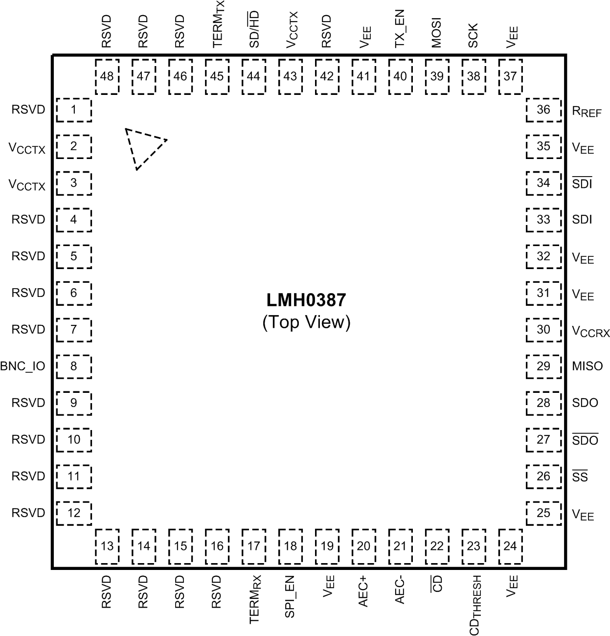
5 Pin Configuration and Functions
NPD Package
48-Pin TLGA
Top View

Pin Functions
| PIN | I/O, TYPE | DESCRIPTION | |
|---|---|---|---|
| NAME | NO. | ||
| AEC+, AEC- | 20, 21 | I/O, Analog | AEC loop filter external capacitor for equalizer (1 µF connected between AEC+ and AEC-). |
| BNC_IO | 8 | I/O, Analog | Serial digital interface input or output for connection to a BNC. Connect this pin to the BNC through an AC coupling capacitor (nominally 4.7 μF). |
| CD | 22 | O, LVCMOS | Carrier detect for BNC_IO pin. H = No input signal detected on BNC_IO pin. L = Input signal detected on BNC_IO pin. |
| CDTHRESH | 23 | I, Analog | Carrier detect threshold input. Sets the threshold for CD. CDTHRESH may be either unconnected or connected to ground for normal CD operation. |
| MISO (SPI) | 29 | O, LVCMOS | SPI Master Input / Slave Output. LMH0387 control data transmit. |
| MOSI (SPI) | 39 | I, LVCMOS | SPI Master Output / Slave Input. LMH0387 control data receive. |
| RREF | 36 | I, Analog | BNC_IO output driver level control. Connect a resistor (nominally 715 Ω) to VCC to set the output voltage swing for the BNC_IO pin. |
| RSVD | 1, 4-7, 9–16, 42, 46-48 | N/A | Do not connect. |
| SCK (SPI) | 38 | I, LVCMOS | SPI serial clock input. |
| SD/HD | 44 | I, LVCMOS | BNC_IO output slew rate control. SD/HD has an internal pulldown. H = BNC_IO output rise/fall time complies with SMPTE 259M (SD). L = BNC_IO output rise/fall time complies with SMPTE 424M / 292M (3G/HD). |
| SDI, SDI | 33, 34 | I, Analog | Serial data differential input for transmitter (cable driver). |
| SDO, SDO | 27, 28 | O, LVDS | Serial data differential output from receiver (equalizer). |
| SPI_EN | 18 | I, LVCMOS | SPI register access enable (equalizer). This pin should always be high; it must be pulled high while operating in the input mode and may optionally be pulled high while operating in the output mode. This pin has an internal pulldown. |
| SS (SPI) | 26 | I, LVCMOS | SPI slave select. This pin has an internal pullup. |
| TERMRX | 17 | I, Analog | Termination for unused receiver (equalizer) input. This network should consist of a 1-µF capacitor followed by a 220-Ω resistor to ground. |
| TERMTX | 45 | O, Analog | Termination for unused transmitter (cable driver) output. This network should consist of a 4.7-µF capacitor followed by a 75-Ω resistor to ground. |
| TX_EN | 40 | I, LVCMOS | Transmitter output driver enable. TX_EN has an internal pullup. H = BNC_IO output driver is enabled. L = BNC_IO output driver is powered off. To configure the LMH0387 as a receiver, the BNC_IO output driver must be disabled by tying TX_EN low. To configure the LMH0387 as a transmitter, the output driver must be enabled by tying TX_EN high and the receiver may be powered down using the sleep mode setting through the SPI. |
| VCCTX | 2, 3, 43 | Power | Positive power supply for transmitter (3.3 V). |
| VEE | 19, 24, 25, 31, 32, 35, 37, 41 | Power | Negative power supply (ground). |
| VCCRX | 30 | Power | Positive power supply for receiver (3.3 V). |