SBOSAF0A april 2023 – august 2023 LMH32401-Q1
PRODUCTION DATA
- 1
- 1 Features
- 2 Applications
- 3 Description
- 4 Revision History
- 5 Pin Configuration and Functions
-
6 Specifications
- 6.1 Absolute Maximum Ratings
- 6.2 ESD Ratings
- 6.3 Recommended Operating Conditions
- 6.4 Thermal Information
- 6.5 Electrical Characteristics: Gain = 2 kΩ
- 6.6 Electrical Characteristics: Gain = 20 kΩ
- 6.7 Electrical Characteristics: Both Gains
- 6.8 Electrical Characteristics: Logic Threshold and Switching Characteristics
- 6.9 Typical Characteristics
- 7 Detailed Description
- 8 Application and Implementation
- 9 Device and Documentation Support
- 10Mechanical, Packaging, and Orderable Information
Package Options
Mechanical Data (Package|Pins)
- RGT|16
Thermal pad, mechanical data (Package|Pins)
- RGT|16
Orderable Information
3 Description
The LMH32401-Q1 automotive device is a programmable-gain, single-ended-input to differential-output transimpedance amplifier for light detection and ranging (LIDAR) applications.
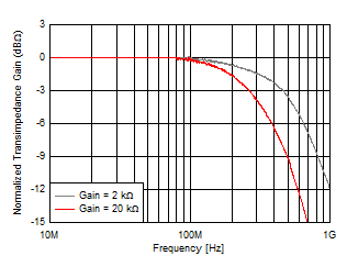
The LMH32401-Q1 can be configured in a gain of 2 kΩ or 20 kΩ. The LMH32401-Q1 has 1.5 VPP of output swing and is designed to drive a 100‑Ω load.
The LMH32401-Q1 has an integrated 100-mA clamp that protects the amplifier and allows the device to rapidly recover from an overloaded input condition. The LMH32401-Q1 also features an integrated ambient-light cancellation circuit. To save board space, as well as reduce system cost, use this circuit instead of ac coupling between the photodiode (PD) or avalanche photodiode (APD) and the amplifier. The ambient-light cancellation circuit can be disabled in cases where dc coupling is required.
To conserve power when the amplifier is not being used, the LMH32401-Q1 provides a low-power mode using the EN pin. When the amplifier is in low-power mode, the output pins are in a high-impedance state. This feature allows several LMH32401-Q1 amplifiers to be multiplexed to a single ADC with the EN control pin serving as the multiplexer select function.
| PART NUMBER | PACKAGE(1) | PACKAGE SIZE(2) |
|---|---|---|
| LMH32401-Q1 | Wettable-flank RGT (VQFN,16) | 3 mm × 3 mm |
 Simplified Block
Diagram
 Closed-Loop Transimpedance
Bandwidth