SBOSA87A December 2021 – November 2022 LMH5485-SEP
PRODUCTION DATA
- 1 Features
- 2 Applications
- 3 Description
- 4 Revision History
- 5 Device Comparison Table
- 6 Pin Configuration and Functions
-
7 Specifications
- 7.1 Absolute Maximum Ratings
- 7.2 ESD Ratings
- 7.3 Recommended Operating Conditions
- 7.4 Thermal Information
- 7.5 Electrical Characteristics: Vs+ – Vs- = 5 V
- 7.6 Electrical Characteristics: Vs+ – Vs- = 3 V
- 7.7 Typical Characteristics: 5 V Single Supply
- 7.8 Typical Characteristics: 3 V Single Supply
- 7.9 Typical Characteristics: 3 V to 5 V Supply Range
- 8 Parameter Measurement Information
- 9 Detailed Description
- 10Application and Implementation
- 11Power Supply Recommendations
- 12Layout
- 13Device and Documentation Support
- 14Mechanical, Packaging, and Orderable Information
Package Options
Mechanical Data (Package|Pins)
- DGK|8
Thermal pad, mechanical data (Package|Pins)
Orderable Information
10.2.1.2 Detailed Design Procedure
Operating the LMH5485-SEP at a low DC noise gain, or with higher feedback resistors, can cause a lower phase margin to exist, giving the response peaking shown in Figure 10-3 for the gain of 0.1 (a 1/10 attenuator) condition. Although it is often useful operating the LMH5485-SEP as an attenuator (taking a large input range to a purely differential signal around a controlled-output, common-mode voltage), the response peaking illustrated in Figure 10-3 is usually undesirable. Several methods can be used to reduce or eliminate this peaking; usually, at the cost of higher output noise. Using DC techniques always increases the output noise broadband, while using an ac noise-gain-shaping technique peaks the noise, but only at higher frequencies that can then be filtered off with the typical passive filters often used after this stage. Figure 10-1 shows a simplified schematic for the gain of 0.1 V/V test from Figure 8-1.
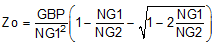
This configuration simulates to a nominal 18° phase margin; therefore, a very highly-peaked response is shown in Figure 10-3. This peaking can be eliminated by placing two feedback capacitors across the Rf elements and a differential input capacitor. Adding these capacitors provides a transition from a resistively set noise gain to a capacitive divider at high-frequency flattening out to a higher noise gain (NG2 here). The key for this approach is to target a Zo, where the noise gain begins to peak up. Using only the following terms, and targeting a closed-loop flat (Butterworth) response, gives this solution sequence for Zo and then the capacitor values.
- Gain bandwidth product in Hz (850 MHz for the LMH5485-SEP)
- Low frequency noise gain, NG1 ( = 1.1 in the attenuator gain of 0.1 V/V design)
- Target high-frequency noise gain selected to be higher than NG1 (NG2 = 3.1 V/V is selected for this design)
- Feedback resistor value, Rf (assumed balanced for this differential design = 402 Ω for this design example)
From these elements, for any decompensated voltage-feedback op amp or FDA, solve for Zo (in Hz) using Equation 1:
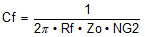
From this target zero frequency in the noise gain, solve for the feedback capacitors using Equation 2:
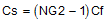
The next step is to resolve the input capacitance on the summing junction. Equation 3 is for a single-ended op amp where that capacitor goes to ground. To use Equation 3 for a voltage-feedback FDA, cut the target value in half, and place the result across the two inputs (reducing the external value by the specified internal differential capacitance).
Setting the external compensation elements using Equation 1 to Equation 3 allows an estimate of the resulting flat bandwidth f–3dB frequency, as shown in Equation 4:
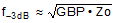
Running through these steps for the LMH5485-SEP in the attenuator circuit of Figure 10-1 gives the proposed compensation of Figure 10-2 where Equation 4 estimates a bandwidth of 252 MHz (Zo target is 74.7 MHz).
The 1 pF across the inputs is really a total 1.9 pF, including the internal differential capacitance. These two designs (with and without the capacitors) were both bench tested and simulated using the LMH5485-SEP TINA model giving the results of Figure 10-3.
This method does a good job of flattening the response for what starts out as a low phase-margin attenuator application. The simulation model does a very good job of predicting the peaking and showing the same improvement with the external capacitors; both giving a flat, approximately 250 MHz, closed-loop bandwidth for this gain of a 0.1 V/V design. In this example, the output noise begins to peak up (as a result of the noise-gain shaping of the capacitors) above 70 MHz. Use postfiltering to minimize any increase in the integrated noise using this technique. Using this solution to deliver an 8 VPP differential output to a successive approximation register (SAR) ADC (using the 2.5 V VOCM shown), the circuit accepts up to ±40 V inputs, where the 4 kΩ input Rg1 draws ±10 mA from the source.