SBOSA33A September 2021 – December 2021 LMH5485-SP
ADVANCE INFORMATION
- 1 Features
- 2 Applications
- 3 Description
- 4 Revision History
- 5 Device Comparison Table
- 6 Pin Configuration and Functions
-
7 Specifications
- 7.1 Absolute Maximum Ratings
- 7.2 ESD Ratings
- 7.3 Recommended Operating Conditions
- 7.4 Thermal Information
- 7.5 Electrical Characteristics: VS+ – VS– = 5 V
- 7.6 Electrical Characteristics: VS+ – VS– = 3 V
- 7.7 Quality Conformance Inspection
- 7.8 Typical Characteristics: 5 V Single Supply
- 7.9 Typical Characteristics: 3 V Single Supply
- 7.10 Typical Characteristics: 3 V to 5 V Supply Range
- 8 Parameter Measurement Information
-
9 Detailed Description
- 9.1 Overview
- 9.2 Functional Block Diagram
- 9.3 Feature Description
- 9.4
Device Functional Modes
- 9.4.1
Operation from Single-Ended Sources to Differential Outputs
- 9.4.1.1 AC-Coupled Signal Path Considerations for Single-Ended Input to Differential Output Conversion
- 9.4.1.2 DC-Coupled Input Signal Path Considerations for Single-Ended to Differential Conversion
- 9.4.1.3 Resistor Design Equations for the Single-Ended to Differential Configuration of the FDA
- 9.4.1.4 Input Impedance for the Single-Ended to Differential FDA Configuration
- 9.4.2 Differential-Input to Differential-Output Operation
- 9.4.1
Operation from Single-Ended Sources to Differential Outputs
- 10Power Supply Recommendations
- 11Layout
- 12Device and Documentation Support
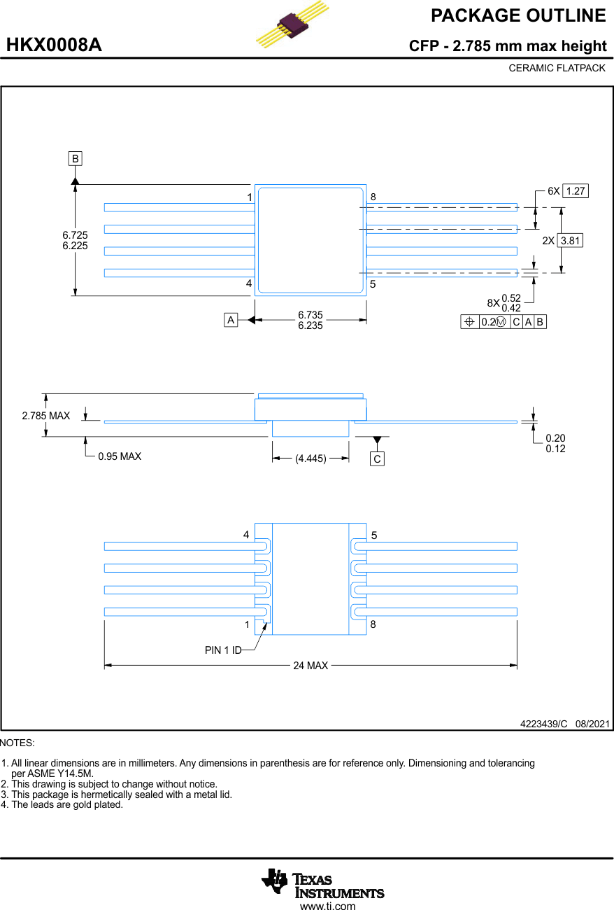
- 13Mechanical, Packaging, and Orderable Information
Package Options
Refer to the PDF data sheet for device specific package drawings
Mechanical Data (Package|Pins)
- HKX|8
Thermal pad, mechanical data (Package|Pins)
Orderable Information
13 Mechanical, Packaging, and Orderable Information
The following pages include mechanical, packaging, and orderable information. This information is the most current data available for the designated devices. This data is subject to change without notice and revision of this document. For browser-based versions of this data sheet, refer to the left-hand navigation.