SNOSB47E May 2011 – August 2016 LMH6521
PRODUCTION DATA.
- 1 Features
- 2 Applications
- 3 Description
- 4 Revision History
- 5 Pin Configuration and Functions
- 6 Specifications
- 7 Detailed Description
- 8 Application and Implementation
- 9 Power Supply Recommendations
- 10Layout
- 11Device and Documentation Support
- 12Mechanical, Packaging, and Orderable Information
Package Options
Mechanical Data (Package|Pins)
- RTV|32
Thermal pad, mechanical data (Package|Pins)
- RTV|32
Orderable Information
1 Features
- OIP3 of 48.5 dBm at 200 MHz
- Maximum Voltage Gain of 26 dB
- Gain Range: 31.5 dB with 0.5-dB Step Size
- Channel Gain Matching of ±0.04 dB
- Noise Figure: 7.3 dB at Maximum Gain
- –3-dB Bandwidth of 1200 MHz
- Low Power Dissipation
- Independent Channel Power Down
- Three Gain Control Modes:
- Parallel Interface
- Serial Interface (SPI)
- Pulse Mode Interface
- Temperature Range: –40°C to +85°C
- Thermally-Enhanced, 32-Pin WQFN Package
2 Applications
- Cellular Base Stations
- Wideband and Narrowband IF Sampling Receivers
- Wideband Direct Conversion
- Digital Pre-Distortion
- ADC Drivers
3 Description
The LMH6521 contains two high performance, digitally controlled variable gain amplifiers (DVGA).
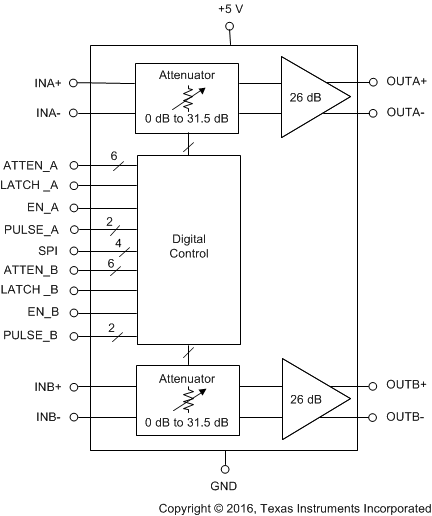
Both channels of the LMH6521 have an independent, digitally controlled attenuator followed by a high linearity, differential output amplifier. Each block has been optimized for low distortion and maximum system design flexibility. Each channel has a high speed power down mode.
The internal digitally controlled attenuator provides precise 0.5-dB gain steps over a 31.5-dB range. Serial and parallel programming options are provided. Serial mode programming uses the SPI interface. A pulse mode is also offered where simple up or down commands can change the gain one step at a time.
The output amplifier has a differential output allowing 10-VPPD signal swings on a single 5-V supply. The low impedance output provides maximum flexibility when driving filters or analog to digital converters.
Device Information(1)
| PART NUMBER | PACKAGE | BODY SIZE (NOM) |
|---|---|---|
| LMH6521 | WQFN (32) | 5.00 mm × 5.00 mm |
- For all available packages, see the orderable addendum at the end of the data sheet.
LMH6521 Block Diagram

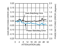
Channel Matching Error (Ch A – Ch B)
