SNOSAK0I December 2004 – January 2015 LMH6550
PRODUCTION DATA.
- 1 Features
- 2 Applications
- 3 Description
- 4 Typical Application Schematic
- 5 Revision History
- 6 Pin Configuration and Functions
- 7 Specifications
- 8 Detailed Description
- 9 Application and Implementation
- 10Power Supply Recommendations
- 11Layout
- 12Device and Documentation Support
- 13Mechanical, Packaging, and Orderable Information
Package Options
Mechanical Data (Package|Pins)
Thermal pad, mechanical data (Package|Pins)
Orderable Information
11 Layout
11.1 Layout Guidelines
The LMH6550 is a very high performance amplifier. To get maximum benefit from the differential circuit architecture, board layout and component selection is very critical. The circuit board should have low a inductance ground plane and well bypassed broad supply lines. External components should be leadless surface mount types. The feedback network and output matching resistors should be composed of short traces and precision resistors (0.1%). The output matching resistors should be placed within 3-4 mm of the amplifier as should the supply bypass capacitors. The LMH730154 evaluation board is an example of good layout techniques.
The LMH6550 is sensitive to parasitic capacitances on the amplifier inputs and to a lesser extent on the outputs as well. Ground and power plane metal should be removed from beneath the amplifier and from beneath RF and RG.
With any differential signal path, symmetry is very important. Even small amounts of asymmetry will contribute to distortion and balance errors.
TI offers evaluation boards to aid in device testing and characterization and as a guide for proper layout. Generally, a good high frequency layout will keep power supply and ground traces away from the inverting input and output pins. Parasitic capacitances on these nodes to ground will cause frequency response peaking and possible circuit oscillations (see OA-15 Frequent Faux Pas in Applying Wideband Current Feedback Amplifiers, SNOA367, for more information).
11.2 Layout Example
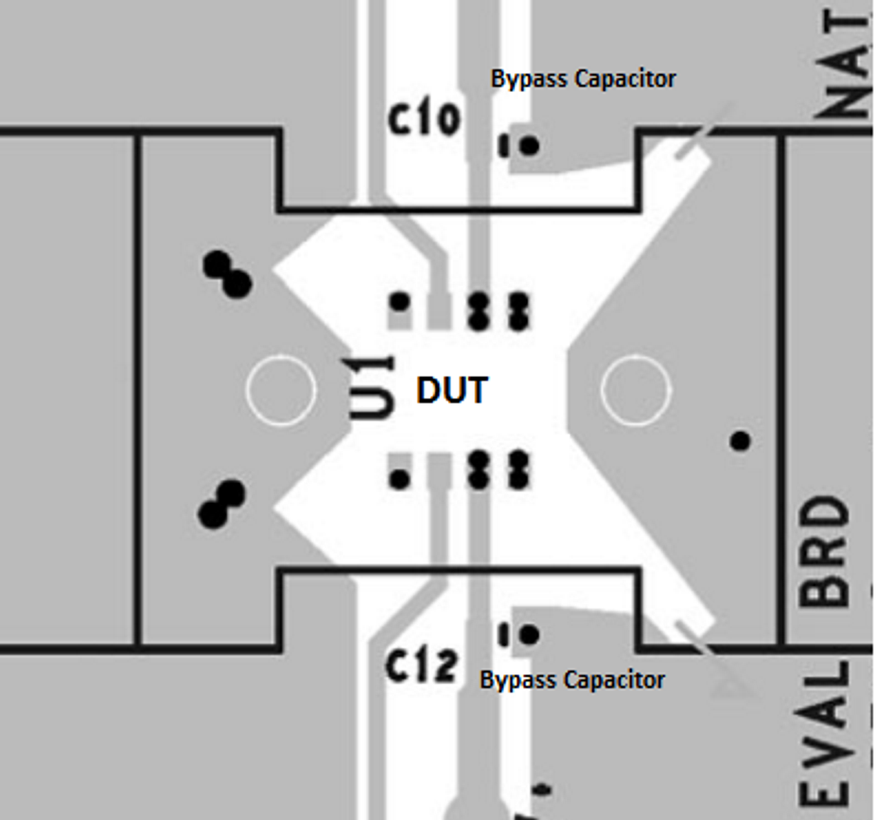 Figure 34. EVM Layout (Top)
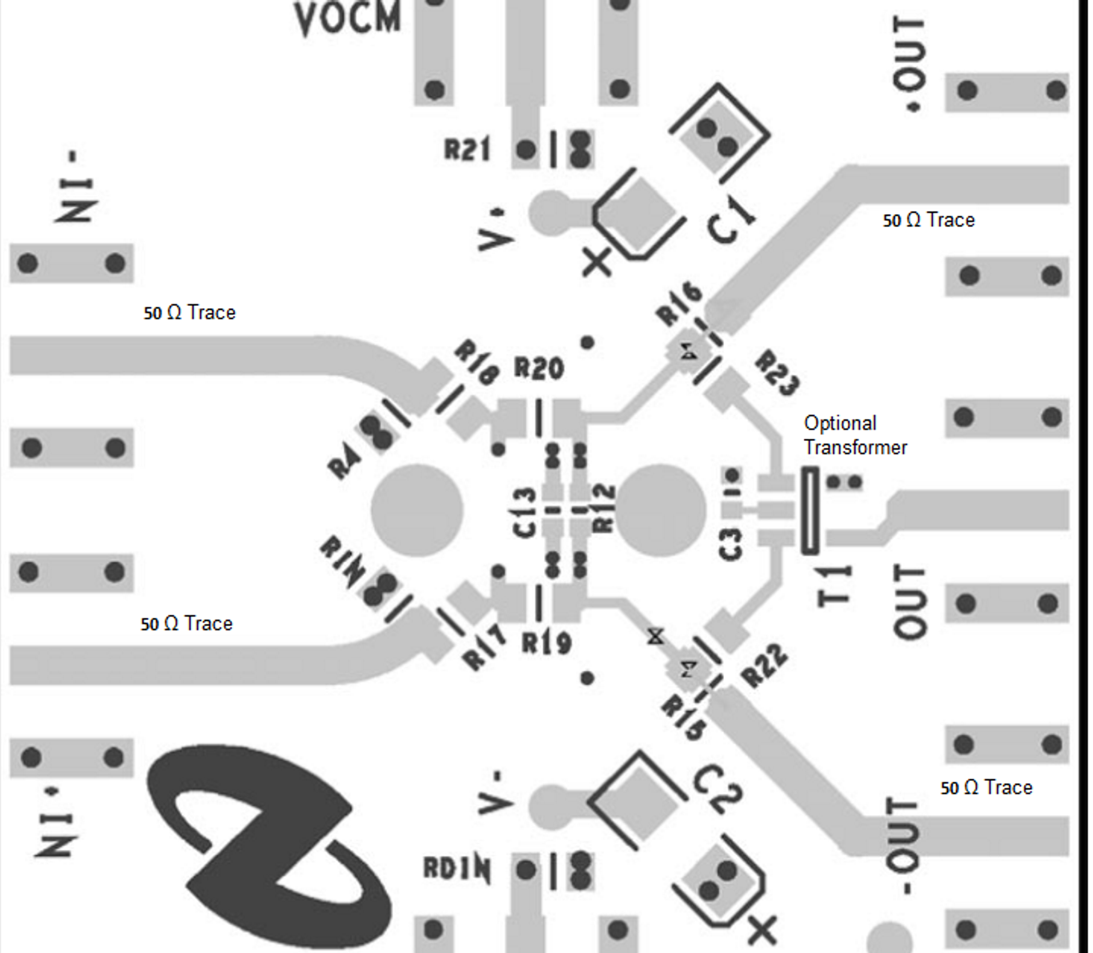 Figure 35. EVM Layout (Bottom)
11.3 Power Dissipation
The LMH6550 is optimized for maximum speed and performance in the small form factor of the standard SOIC package, and is essentially a dual channel amplifier. To ensure maximum output drive and highest performance, thermal shutdown is not provided. Therefore, it is of utmost importance to make sure that the TJMAX of 150°C is never exceeded due to the overall power dissipation.
Follow these steps to determine the Maximum power dissipation for the LMH6550:
- Calculate the quiescent (no-load) power: PAMP = ICC* (VS), where VS = V+ - V−. (Be sure to include any current through the feedback network if VOCM is not mid rail.)
- Calculate the RMS power dissipated in each of the output stages: PD (rms) = rms ((VS - V+OUT) * I+OUT) + rms ((VS − V−OUT) * I−OUT), where VOUT and IOUT are the voltage and the current measured at the output pins of the differential amplifier as if they were single-ended amplifiers and VS is the total supply voltage.
- Calculate the total RMS power: PT = PAMP + PD.
The maximum power that the LMH6550 package can dissipate at a given temperature can be derived with the following equation:
where
- TAMB = Ambient temperature (°C)
- θJA = Thermal resistance, from junction to ambient, for a given package (°C/W)
- For the SOIC package θJA is 150°C/W
- For the VSSOP package θJA is 235°C/W
NOTE
If VCM is not 0V then there will be quiescent current flowing in the feedback network. This current should be included in the thermal calculations and added into the quiescent power dissipation of the amplifier.
11.4 ESD Protection
The LMH6550 is protected against electrostatic discharge (ESD) on all pins. The LMH6550 will survive 2000 V Human Body model and 200 V Machine model events. Under normal operation the ESD diodes have no effect on circuit performance. There are occasions, however, when the ESD diodes will be evident. If the LMH6550 is driven by a large signal while the device is powered down the ESD diodes will conduct. The current that flows through the ESD diodes will either exit the chip through the supply pins or will flow through the device, hence it is possible to power up a chip with a large signal applied to the input pins. Using the shutdown mode is one way to conserve power and still prevent unexpected operation.