SNOSAK7D February 2005 – January 2015 LMH6551
PRODUCTION DATA.
- 1 Features
- 2 Applications
- 3 Description
- 4 Typical Application
- 5 Revision History
- 6 Pin Configuration and Functions
- 7 Specifications
- 8 Detailed Description
- 9 Application and Implementation
- 10Power Supply Recommendations
- 11Layout
- 12Device and Documentation Support
- 13Mechanical, Packaging, and Orderable Information
Package Options
Mechanical Data (Package|Pins)
Thermal pad, mechanical data (Package|Pins)
Orderable Information
7 Specifications
7.1 Absolute Maximum Ratings (1)(2)(3)
| MIN | MAX | UNIT | |
|---|---|---|---|
| Supply Voltage | 13.2 | V | |
| Common-Mode Input Voltage | ±Vs | V | |
| Maximum Input Current (pins 1, 2, 7, 8) | 30 | mA | |
| Maximum Output Current (pins 4, 5) | See (2) | ||
| Maximum Junction Temperature | 150 | °C | |
| Storage Temperature, Tstg | −65 | 150 | °C |
(1) Absolute Maximum Ratings indicate limits beyond which damage to the device may occur. Recommended Operating Conditions indicate conditions for which the device is intended to be functional, but specific performance is not ensured. For ensured specifications, see the Electrical Characteristics tables.
(2) If Military/Aerospace specified devices are required, please contact the Texas Instruments Sales Office/ Distributors for availability and specifications.
(3) For Soldering Information, see Product Folder at www.ti.com and SNOA549.
7.2 ESD Ratings
| VALUE | UNIT | |||
|---|---|---|---|---|
| V(ESD) | Electrostatic discharge | Human-body model (HBM), per ANSI/ESDA/JEDEC JS-001(1) | ±2000 | V |
| Machine model (MM) | ±200 | |||
(1) JEDEC document JEP155 states that 500-V HBM allows safe manufacturing with a standard ESD control process.
7.3 Recommended Operating Conditions
| MIN | NOM | MAX | UNIT | |
|---|---|---|---|---|
| Operating Temperature Range | −40 | +125 | °C | |
| Total Supply Voltage | 3 | 12 | V |
7.4 Thermal Information
| THERMAL METRIC(1) | LMH6551 | UNIT | ||
|---|---|---|---|---|
| D | DGK | |||
| 8 PINS | 8 PINS | |||
| RθJA | Junction-to-ambient thermal resistance (3) | 150 | 235 | °C/W |
(1) For more information about traditional and new thermal metrics, see the IC Package Thermal Metrics application report, SPRA953.
7.5 Electrical Characteristics: ±5 V(1)
Single-ended in differential out, TA= 25°C, G = +1, VS = ±5 V, VCM = 0 V, RF = RG = 365 Ω, RL = 500 Ω; unless specified.| PARAMETER | TEST CONDITIONS | MIN (6) | TYP (5) | MAX (6) | UNIT | ||
|---|---|---|---|---|---|---|---|
| AC PERFORMANCE (DIFFERENTIAL) | |||||||
| SSBW | Small Signal −3 dB Bandwidth | VOUT = 0.5 VPP | 370 | MHz | |||
| LSBW | Large Signal −3 dB Bandwidth | VOUT = 2 VPP | 340 | MHz | |||
| Large Signal −3 dB Bandwidth | VOUT = 4 VPP | 320 | MHz | ||||
| 0.1 dB Bandwidth | VOUT = 2 VPP | 50 | MHz | ||||
| Slew Rate | 4-V Step(4) | 2400 | V/μs | ||||
| Rise/Fall Time | 2-V Step | 1.8 | ns | ||||
| Settling Time | 2-V Step, 0.05% | 18 | ns | ||||
| VCM PIN AC PERFORMANCE (COMMON-MODE FEEDBACK AMPLIFIER) | |||||||
| Common-Mode Small Signal Bandwidth | VCMbypass capacitor removed | 200 | MHz | ||||
| DISTORTION AND NOISE RESPONSE | |||||||
| HD2 | VO = 2 VPP, f = 5 MHz, RL=800 Ω | −94 | dBc | ||||
| HD2 | VO = 2 VPP, f = 20MHz, RL=800 Ω | −85 | dBc | ||||
| HD3 | VO = 2 VPP, f = 5 MHz, RL=800 Ω | −96 | dBc | ||||
| HD3 | VO = 2 VPP, f = 20 MHz, RL=800 Ω | −72 | dBc | ||||
| en | Input Referred Voltage Noise | Freq ≥ 1 MHz | 6.0 | nV/√Hz | |||
| in | Input Referred Noise Current | Freq ≥ 1 MHz | 1.5 | pA/√Hz | |||
| INPUT CHARACTERISTICS (DIFFERENTIAL) | |||||||
| VOSD | Input Offset Voltage | Differential Mode, VID = 0, VCM = 0 | 0.5 | ±4 | mV | ||
| At extreme temperatures | ±6 | ||||||
| Input Offset Voltage Average Temperature Drift(8) | −0.8 | µV/°C | |||||
| IBI | Input Bias Current(7) | -4 | 0 -10 |
µA | |||
| Input Bias Current Average Temperature Drift(8) | −2.6 | nA/°C | |||||
| Input Bias Difference | Difference in Bias currents between the two inputs | 0.03 | µA | ||||
| CMRR | Common-Mode Rejection Ratio | DC, VCM = 0 V, VID = 0 V | 72 | 80 | dBc | ||
| RIN | Input Resistance | Differential | 5 | MΩ | |||
| CIN | Input Capacitance | Differential | 1 | pF | |||
| CMVR | Input Common-Mode Voltage Range | CMRR > 53dB | +3.1 −4.6 |
+3.2 −4.7 |
V | ||
| VCMPIN INPUT CHARACTERISTICS (COMMON-MODE FEEDBACK AMPLIFIER) | |||||||
| VOSC | Input Offset Voltage | Common Mode, VID = 0 | 0.5 | ±5 | mV | ||
| At extreme temperatures | ±8 | ||||||
| Input Offset Voltage Average Temperature Drift(8) | 8.2 | µV/°C | |||||
| Input Bias Current(7) | −2 | μA | |||||
| VCM CMRR | VID = 0 V, 1-V step on VCM pin, measure VOD | 70 | 75 | dB | |||
| Input Resistance | 25 | kΩ | |||||
| Common-Mode Gain | ΔVO,CM/ΔVCM | 0.995 | 0.999 | 1.005 | V/V | ||
| OUTPUT PERFORMANCE | |||||||
| Output Voltage Swing | Single-Ended, Peak to Peak | ±7.38 | ±7.8 | V | |||
| At extreme temperatures | ±7.18 | ||||||
| Output Common-Mode Voltage Range | VID = 0 V, | ±3.69 | ±3.8 | V | |||
| IOUT | Linear Output Current | VOUT = 0V | ±50 | ±65 | mA | ||
| ISC | Short Circuit Current | Output Shorted to Ground VIN = 3-V Single-Ended(2)l |
140 | mA | |||
| Output Balance Error | ΔVOUTCommon Mode /ΔVOUTDIfferential , VOUT = 0.5 Vpp Differential, f = 10 MHz | −70 | dB | ||||
| MISCELLANEOUS PERFORMANCE | |||||||
| AVOL | Open Loop Gain | Differential | 70 | dB | |||
| PSRR | Power Supply Rejection Ratio | DC, ΔVS = ±1 V | 74 | 90 | dB | ||
| Supply Current | RL = ∞ | 11 | 12.5 | 14.5 | mA | ||
| At extreme temperatures | 16.5 | ||||||
7.6 Electrical Characteristics: 5 V(1)
Single-ended in differential out, TA= 25°C, G = +1, VS = 5 V, VCM = 2.5 V, RF = RG = 365 Ω, RL = 500 Ω; unless specified.| PARAMETER | TEST CONDITIONS | MIN (6) | TYP (5) | MAX (6) | UNIT | ||
|---|---|---|---|---|---|---|---|
| SSBW | Small Signal −3 dB Bandwidth | RL = 500 Ω, VOUT = 0.5 VPP | 350 | MHz | |||
| LSBW | Large Signal −3 dB Bandwidth | RL = 500 Ω, VOUT = 2 VPP | 300 | MHz | |||
| 0.1 dB Bandwidth | VOUT = 2 VPP | 50 | MHz | ||||
| Slew Rate | 4-V Step(4) | 1800 | V/μs | ||||
| Rise/Fall Time, 10% to 90% | 4-V Step | 2 | ns | ||||
| Settling Time | 4-V Step, 0.05% | 17 | ns | ||||
| VCM PIN AC PERFORMANCE (COMMON-MODE FEEDBACK AMPLIFIER) | |||||||
| Common-Mode Small Signal Bandwidth | 170 | MHz | |||||
| DISTORTION AND NOISE RESPONSE | |||||||
| HD2 | 2nd Harmonic Distortion | VO = 2 VPP, f = 5 MHz, RL=800 Ω | −84 | dBc | |||
| HD2 | VO = 2 VPP, f = 20 MHz, RL=800 Ω | −69 | dBc | ||||
| HD3 | 3rd Harmonic Distortion | VO = 2 VPP, f = 5 MHz, RL=800 Ω | −93 | dBc | |||
| HD3 | VO = 2 VPP, f = 20 MHz, RL=800 Ω | −67 | dBc | ||||
| en | Input Referred Noise Voltage | Freq ≥ 1 MHz | 6.0 | nV/√Hz | |||
| in | Input Referred Noise Current | Freq ≥ 1 MHz | 1.5 | pA/√Hz | |||
| INPUT CHARACTERISTICS (DIFFERENTIAL) | |||||||
| VOSD | Input Offset Voltage | Differential Mode, VID = 0, VCM = 0 | 0.5 | ±4 | mV | ||
| At extreme temperatures | ±6 | ||||||
| Input Offset Voltage Average Temperature Drift(8) | −0.8 | µV/°C | |||||
| IBIAS | Input Bias Current(7) | −4 | 0 -10 |
μA | |||
| Input Bias Current Average Temperature Drift(8) | −3 | nA/°C | |||||
| Input Bias Current Difference | Difference in Bias currents between the two inputs | 0.03 | µA | ||||
| CMRR | Common-Mode Rejection Ratio | DC, VID = 0 V | 70 | 78 | dBc | ||
| Input Resistance | Differential | 5 | MΩ | ||||
| Input Capacitance | Differential | 1 | pF | ||||
| VICM | Input Common-Mode Range | CMRR > 53 dB | +3.1 +0.4 |
+3.2 +0.3 |
|||
| VCMPIN INPUT CHARACTERISTICS (COMMON-MODE FEEDBACK AMPLIFIER) | |||||||
| Input Offset Voltage | Common Mode, VID = 0 | 0.5 | ±5 | mV | |||
| At extreme temperatures | ±8 | ||||||
| Input Offset Voltage Average Temperature Drift | 5.8 | µV/°C | |||||
| Input Bias Current | 3 | μA | |||||
| VCM CMRR | VID = 0, 1V step on VCM pin, measure VOD |
70 | 75 | dB | |||
| Input Resistance | VCM pin to ground | 25 | kΩ | ||||
| Common-Mode Gain | ΔVO,CM/ΔVCM | 0.995 | 0.991 | 1.005 | V/V | ||
| OUTPUT PERFORMANCE | |||||||
| VOUT | Output Voltage Swing | Single-Ended, Peak to Peak, VS= ±2.5 V, VCM= 0 V | ±2.4 | ±2.8 | V | ||
| IOUT | Linear Output Current | VOUT = 0-V Differential | ±45 | ±60 | mA | ||
| ISC | Output Short Circuit Current | Output Shorted to Ground VIN = 3-V Single-Ended(2) |
230 | mA | |||
| CMVR | Output Common-Mode Voltage Range | VID = 0, VCMpin = 1.2 V and 3.8 V | 3.72 1.23 |
3.8 1.2 |
V | ||
| Output Balance Error | ΔVOUTCommon Mode /ΔVOUTDIfferential, VOUT = 1Vpp Differential, f = 10 MHz | −65 | dB | ||||
| MISCELLANEOUS PERFORMANCE | |||||||
| Open Loop Gain | DC, Differential | 70 | dB | ||||
| PSRR | Power Supply Rejection Ratio | DC, ΔVS = ±0.5 V | 72 | 88 | dB | ||
| IS | Supply Current | RL = ∞ | 10 | 11.5 | 13.5 | mA | |
| At extreme temperatures | 15.5 | ||||||
7.7 Electrical Characteristics: 3.3 V(1)
Single-ended in differential out, TA= 25°C, G = +1, VS = 3.3 V, VCM = 1.65 V, RF = RG = 365 Ω, RL = 500 Ω; unless specified.| PARAMETER | TEST CONDITIONS | MIN (6) | TYP (5) | MAX (6) | UNIT | |
|---|---|---|---|---|---|---|
| SSBW | Small Signal −3 dB Bandwidth | RL = 500 Ω, VOUT = 0.5 VPP | 320 | MHz | ||
| LSBW | Large Signal −3 dB Bandwidth | RL = 500 Ω, VOUT = 1 VPP | 300 | MHz | ||
| Slew Rate | 1-V Step(4) | 700 | V/μs | |||
| Rise/Fall Time, 10% to 90% | 1-V Step | 2 | ns | |||
| VCM PIN AC PERFORMANCE (COMMON-MODE FEEDBACK AMPLIFIER) | ||||||
| Common-Mode Small Signal Bandwidth | 95 | MHz | ||||
| DISTORTION AND NOISE RESPONSE | ||||||
| HD2 | 2nd Harmonic Distortion | VO = 1 VPP, f = 5 MHz, RL=800 Ω | −93 | dBc | ||
| HD2 | VO = 1 VPP, f = 20 MHz, RL=800 Ω | −74 | dBc | |||
| HD3 | 3rd Harmonic Distortion | VO = 1 VPP, f = 5 MHz, RL=800 Ω | −85 | dBc | ||
| HD3 | VO = 1 VPP, f = 20 MHz, RL=800 Ω | −69 | dBc | |||
| INPUT CHARACTERISTICS (DIFFERENTIAL) | ||||||
| VOSD | Input Offset Voltage | Differential Mode, VID = 0, VCM = 0 | 1 | mV | ||
| Input Offset Voltage Average Temperature Drift(8) | 1.6 | µV/°C | ||||
| IBIAS | Input Bias Current(7) | −8 | μA | |||
| Input Bias Current Average Temperature Drift(8) | 9.5 | nA/°C | ||||
| Input Bias Current Difference | Difference in Bias currents between the two inputs | 0.3 | µA | |||
| CMRR | Common-Mode Rejection Ratio | DC, VID = 0 V | 78 | dBc | ||
| Input Resistance | Differential | 5 | MΩ | |||
| Input Capacitance | Differential | 1 | pF | |||
| VICM | Input Common-Mode Range | CMRR > 53 dB | +1.5 +0.3 |
|||
| VCMPIN INPUT CHARACTERISTICS (COMMON-MODE FEEDBACK AMPLIFIER) | ||||||
| Input Offset Voltage | Common Mode, VID = 0 | 1 | ±5 | mV | ||
| Input Offset Voltage Average Temperature Drift | 18.6 | µV/°C | ||||
| Input Bias Current | 3 | μA | ||||
| VCM CMRR | VID = 0, 1-V step on VCM pin, measure VOD |
60 | dB | |||
| Input Resistance | VCM pin to ground | 25 | kΩ | |||
| Common-Mode Gain | ΔVO,CM/ΔVCM | 0.999 | V/V | |||
| OUTPUT PERFORMANCE | ||||||
| VOUT | Output Voltage Swing | Single-Ended, Peak to Peak, VS= 3.3 V, VCM= 1.65 V | ±0.75 | ±0.9 | V | |
| IOUT | Linear Output Current | VOUT = 0-V Differential | ±30 | ±40 | mA | |
| ISC | Output Short Circuit Current | Output Shorted to Ground VIN = 2-V Single-Ended(2) |
200 | mA | ||
| CMVR | Output Common-Mode Voltage Range | VID = 0, VCMpin = 1.2 V and 2.1 V | 2.1 1.2 |
V | ||
| Output Balance Error | ΔVOUTCommon Mode /ΔVOUTDIfferential, VOUT = 1-Vpp Differential, f = 10 MHz | −65 | dB | |||
| MISCELLANEOUS PERFORMANCE | ||||||
| Open Loop Gain | DC, Differential | 70 | dB | |||
| PSRR | Power Supply Rejection Ratio | DC, ΔVS = ±0.5 V | 75 | dB | ||
| IS | Supply Current | RL = ∞ | 8 | mA | ||
(1) Electrical Table values apply only for factory testing conditions at the temperature indicated. Factory testing conditions result in very limited self-heating of the device such that TJ = TA. No specification of parametric performance is indicated in the electrical tables under conditions of internal self-heating where TJ > TA.
(2) The maximum output current (IOUT) is determined by device power dissipation limitations.
(3) The maximum power dissipation is a function of TJ(MAX), θJA and TA. The maximum allowable power dissipation at any ambient temperature is P D= (TJ(MAX) — TA)/ θJA. All numbers apply for package soldered directly into a 2 layer PC board with zero air flow.
(4) Slew Rate is the average of the rising and falling edges.
(5) Typical numbers are the most likely parametric norm.
(6) Limits are 100% production tested at 25°C. Limits over the operating temperature range are specified through correlation using Statistical Quality Control (SQC) methods.
(7) Negative input current implies current flowing out of the device.
(8) Drift determined by dividing the change in parameter at temperature extremes by the total temperature change.
7.8 Typical Performance Characteristics
(TA = 25°C, VS = ±5 V, RL = 500 Ω, RF = RG = 365 Ω; Unless Specified).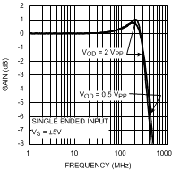 Figure 1. Frequency Response vs Supply Voltage
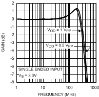 Figure 3. Frequency Response vs VOUT
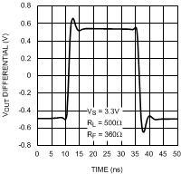 Figure 5. 1 VPP Pulse Response Single-Ended Input
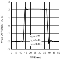 Figure 7. Large Signal Pulse Response
 Figure 9. Distortion vs Frequency
 Figure 11. Distortion vs Frequency
 Figure 13. Distortion vs Supply Voltage (Single Supply)
 Figure 15. Minimum VOUT vs IOUT
 Figure 17. Closed-Loop Output Impedance
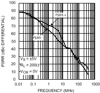 Figure 19. PSRR
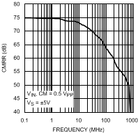 Figure 21. CMRR
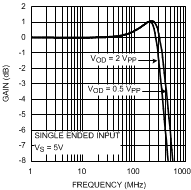 Figure 2. Frequency Response
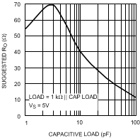 Figure 4. Suggested ROUT vs Cap Load
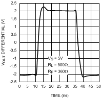 Figure 6. 2 VPP Pulse Response Single-Ended Input
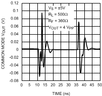 Figure 8. Output Common-Mode Pulse Response
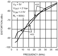 Figure 10. Distortion vs Frequency
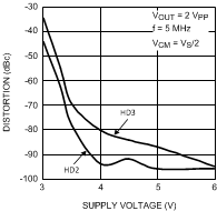 Figure 12. Distortion vs Supply Voltage (Split Supplies)
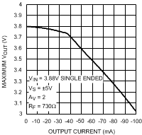 Figure 14. Maximum VOUT vs IOUT
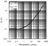 Figure 16. Closed-Loop Output Impedance
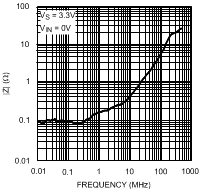 Figure 18. Closed-Loop Output Impedance
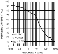 Figure 20. PSRR
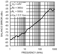 Figure 22. Balance Error