SNOS957H April 2001 – August 2014 LMH6672
PRODUCTION DATA.
- 1 Features
- 2 Applications
- 3 Description
- 4 Revision History
- 5 Pin Configuration and Functions
- 6 Specifications
- 7 Detailed Description
- 8 Power Supply Recommendations
- 9 Device and Documentation Support
- 10Mechanical, Packaging, and Orderable Information
Package Options
Mechanical Data (Package|Pins)
Thermal pad, mechanical data (Package|Pins)
- DDA|8
Orderable Information
6 Specifications
6.1 Absolute Maximum Ratings(1)
over operating free-air temperature range (unless otherwise noted)| MIN | MAX | UNIT | ||
|---|---|---|---|---|
| VIN Differential | ±1.2 | V | ||
| Output Short Circuit Duration | See(2) | |||
| Supply Voltage (V+ − V−) | 13.2 | V | ||
| Voltage at Input/Output pins | V+ +0.8 V− −0.8 |
V | ||
| Junction Temperature | +150(3) | °C | ||
| Soldering Information | Infrared or Convection (20 sec) | 235 | °C | |
| Wave Soldering (10 sec) | 260 | °C | ||
(1) Stresses beyond those listed under Absolute Maximum Ratings may cause permanent damage to the device. These are stress ratings only, which do not imply functional operation of the device at these or any other conditions beyond those indicated under Recommended Operating Conditions. Exposure to absolute-maximum-rated conditions for extended periods may affect device reliability.
6.2 Handling Ratings
| MIN | MAX | UNIT | |||
|---|---|---|---|---|---|
| Tstg | Storage temperature range | −65 | +150 | °C | |
| V(ESD) | Electrostatic discharge(1) | Human body model (HBM), per ANSI/ESDA/JEDEC JS-001, all pins(1) | 2 | 2000 | V |
| Machine Model (MM)l(2) | 200 | ||||
(1) JEDEC document JEP155 states that 2000-V HBM allows safe manufacturing with a standard ESD control process.
(2) JEDEC document JEP157 states that 200-V MM allows safe manufacturing with a standard ESD control process.
6.3 Recommended Operating Conditions
over operating free-air temperature range (unless otherwise noted)| MIN | MAX | UNIT | |
|---|---|---|---|
| Supply Voltage (V+ - V−) | ±2.5 | ±6.5 | V |
| Operating Temperature Range | −40 | 150 | °C |
6.4 Thermal Information
| THERMAL METRIC(1) | SOIC Package D |
SO PowerPAD Package DDA |
UNIT | |
|---|---|---|---|---|
| 8 PINS | 8 PINS | |||
| RθJA | Junction-to-ambient thermal resistance | 172 | 58.6 | °C/W |
(1) For more information about traditional and new thermal metrics, see the IC Package Thermal Metrics application report, SPRA953.
6.5 Electrical Characteristics
Unless otherwise specified, all limits are ensured for G = +2, VS = ±2.5 to ±6V, RF = RIN = 470Ω, RL = 100Ω.| PARAMETER | TEST CONDITIONS | MIN(5) | TYP(4) | MAX(5) | UNIT | |
|---|---|---|---|---|---|---|
| DYNAMIC PERFORMANCE | ||||||
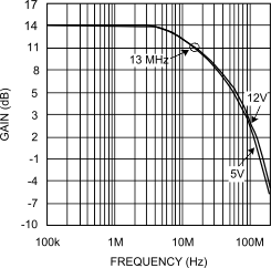
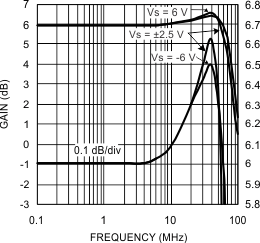
| −3dB Bandwidth | 90 | MHz | ||||
| 0.1dB Bandwidth | VS = ±6V | 12 | MHz | |||
| Slew Rate | VS = ±6V, 4V Step, 10-90% | 135 | V/μs | |||
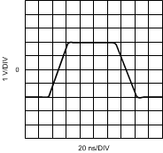
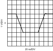
| Rise and Fall Time | VS = 6V, 4V Step, 10-90% | 23.5 | ns | |||
| DISTORTION and NOISE RESPONSE | ||||||
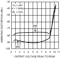
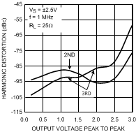
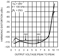
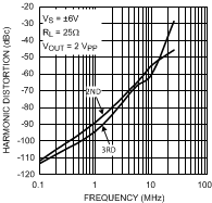
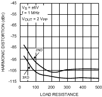
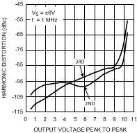
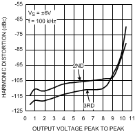
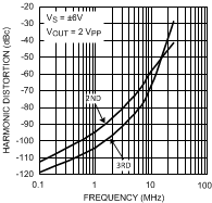
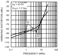
| 2nd Harmonic Distortion | VO = 8.4 VPP, f = 100 kHz, RL = 25Ω | −105 | dBc | |||
| VO = 8.4 VPP, f = 1 MHz, RL = 100Ω | −90 | dBc | ||||
| 3rd Harmonic Distortion | VO = 8.4 VPP, f = 100 kHz, RL = 25Ω | −110 | dBc | |||
| VO = 8.4 VPP, f = 1 MHz, RL = 100Ω | −87 | dBc | ||||
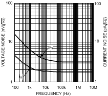
| Input Noise Voltage | f = 100 kHz | 3.1 | nV√Hz | |||
| Input Noise Current | f = 100 kHz | 1.8 | pA/√Hz | |||
| INPUT CHARACTERISTICS | ||||||
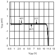
| VOS | Input Offset Voltage | TJ = −40°C to 125°C | −5.5 | 0.1 | 5.5 | mV |
| −4 | −0.2 | 4 | ||||
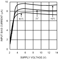
| IB | Input Bias Current | TJ = −40°C to 125°C | 8 | 16 | µA | |
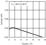
| IOS | Input Offset Current | TJ = −40°C to 125°C | −2.1 | 0 | 2.1 | µA |
| CMVR | Common Voltage Range | VS = ±6V | −6.0 | −5.7 to 4.5 | 4.5 | V |
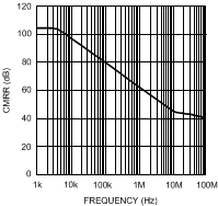
| CMRR | Common-Mode Rejection Ratio | VS = ±6V, TJ = −40°C to 125°C | 150 | 7.5 | µV/V | |
| TRANSFER CHARACTERISTICS | ||||||
| AVOL | Voltage Gain | RL = 1k, TJ = −40°C to 125°C | 1.0 | 5 | V/mV | |
| RL = 25Ω, TJ = −40°C to 125°C | 0.67 | 3.4 | V/mV | |||
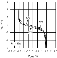
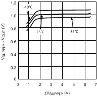
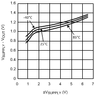
| VO | Output Swing | RL = 25Ω, VS = ±6V | −4.5 | ±4.8 | 4.5 | V |
| RL = 25Ω, TJ = −40°C to 125°C, VS = ±6V |
−4.4 | ±4.8 | 4.4 | |||
| VO | Output Swing | RL = 1k, VS = ±6V | −4.8 | ±4.8 | 4.8 | V |
| RL = 1k, TJ = −40°C to 125°C, VS = ±6V |
−4.7 | ±4.8 | 4.7 | |||
| ISC | Output Current(2) | VO = 0, VS = ±6V | 350 | 525 | mA | |
| VO = 0, VS = ±6V, TJ = −40°C to 125°C |
260 | 600 | mA | |||
| POWER SUPPLY | ||||||
| IS | Supply Current/Amp | VS = ±6V | 8 | mA | ||
| VS = ±6V, TJ = −40°C to 125°C | 7.2 | 9 | ||||
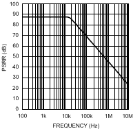
| PSRR | Power Supply Rejection Ratio | VS = ±2.5V to ±6V, TJ = −40°C to 125°C |
72 | 88.5 | dB | |
6.6 ±2.5V Electrical Characteristics
Unless otherwise specified, all limits are ensured for G = +2, VS = ±2.5 to ±6V, RF = RIN = 470Ω, RL = 100Ω.| PARAMETER | TEST CONDITIONS | MIN(5) | TYP(4) | MAX(5) | UNIT | |
|---|---|---|---|---|---|---|
| DYNAMIC PERFORMANCE | ||||||
| −3 dB Bandwidth | 80 | MHz | ||||
| 0.1 dB Bandwidth | 12 | MHz | ||||
| Rise and Fall Time | 2V Step, 10-90% | 14 | ns | |||
| DISTORTION and NOISE RESPONSE | ||||||
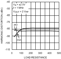
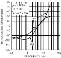
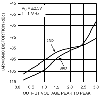
| 2nd Harmonic Distortion | VO = 2 VPP, f = 100 kHz, RL = 25Ω | −96 | dBc | |||
| VO = 2 VPP, f = 1 MHz, RL = 100Ω | −85 | dBc | ||||
| 3rd Harmonic Distortion | VO = 2 VPP, f = 100 kHz, RL = 25Ω | −98 | dBc | |||
| VO = 2 VPP, f = 1 MHz, RL = 100Ω | −87 | dBc | ||||
| INPUT CHARACTERISTICS | ||||||
| VOS | Input Offset Voltage | TJ = −40°C to 125°C | −5.5 | 5.5 | mV | |
| −4.0 | 0.02 | 4.0 | ||||
| IB | Input Bias Current | TJ = −40°C to 125°C | 8.0 | 16 | µA | |
| CMVR | Common-Mode Voltage Range | −2.5 | 1.0 | V | ||
| CMRR | Common-Mode Rejection Ratio | TJ = −40°C to 125°C | 150 | 8 | µV/V | |
| TRANSFER CHARACTERISTICS | ||||||
| AVOL | Voltage Gain | RL = 25Ω, TJ = −40°C to 125°C | 0.67 | 3 | V/mV | |
| RL = 1k, TJ = −40°C to 125°C | 1.0 | 4 | ||||
| OUTPUT CHARACTERISTICS | ||||||
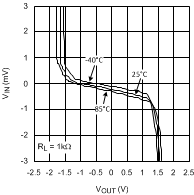
| VO | Output Voltage Swing | RL = 25Ω | 1.20 | 1.45 | V | |
| RL = 25Ω, TJ = −40°C to 125°C | 1.10 | 1.35 | ||||
| RL = 1k | 1.30 | 1.60 | ||||
| RL = 1k, TJ = −40°C to 125°C | 1.25 | 1.50 | ||||
| POWER SUPPLY | ||||||
| IS | Supply Current/Amp | 8.0 | mA | |||
| TJ = −40°C to 125°C | 6.7 | 9.0 | ||||
(1) Human body model, 1.5 kΩ in series with 100 pF. Machine model, 200 Ω in series with 100 pF.
(2) Shorting the output to either supply or ground will exceed the absolute maximum TJ and can result in failure.
(3) The maximum power dissipation is a function of TJ(MAX), RθJA and TA. The maximum allowable power dissipation at any ambient temperature is PD = (TJ(MAX) − TA)/RθJA. All numbers apply for packages soldered directly onto a PC board.
(4) Typical values represent the most likely parametric norm.
(5) All limits are specified by testing, characterization or statistical analysis.
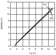
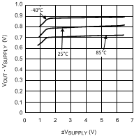
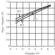
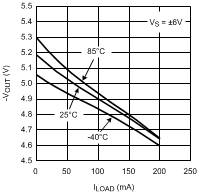
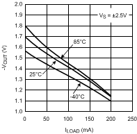
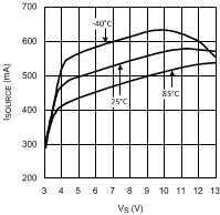
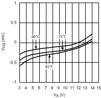
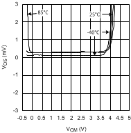
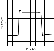
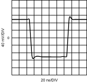
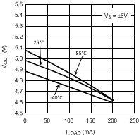
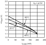
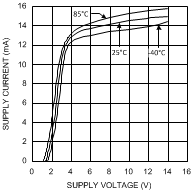
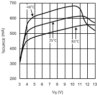
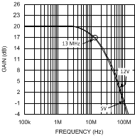
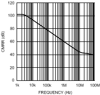
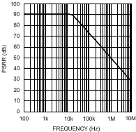
6.7 Typical Performance Characteristics
Av = + 2V/V