SNOSAW6E January 2008 – December 2014 LMP7721
PRODUCTION DATA.
- 1 Features
- 2 Applications
- 3 Description
- 4 Revision History
- 5 Pin Configuration and Functions
- 6 Specifications
- 7 Detailed Description
- 8 Application and Implementation
- 9 Power Supply Recommendations
- 10Layout
- 11Device and Documentation Support
- 12Mechanical, Packaging, and Orderable Information
Package Options
Mechanical Data (Package|Pins)
- D|8
Thermal pad, mechanical data (Package|Pins)
Orderable Information
7 Detailed Description
7.1 Overview
The LMP7721 combines a patented input bias current cancelling circuitry along with an optimized pinout to provide and ultra-low maximum specified bias current of ±20 fA.
7.2 Functional Block Diagram
7.3 Feature Description
7.3.1 Ultra-Low Input Bias Current
The LMP7721 has the industry’s lowest specified input bias current. The ultra-low input bias current is typically 3 fA, with a specified limit of ±20 fA at 25°C, ±900 fA at 85°C and ±5 pA at 125°C when VCM = 1 V with a 5-V or a 2.5-V power supply.
7.3.2 Wide Bandwidth at Low-Supply Current
The LMP7721 is a high-performance amplifier that provides a 17-MHz unity gain bandwidth while drawing only 1.3 mA of current. This makes the LMP7721 ideal for wideband amplification in portable applications.
7.3.3 Low Input Referred Noise
The LMP7721 has a low input-referred voltage noise density (6.5 nV at 1 kHz with 5-V supply). Its MOS input stage ensures a very low input-referred current noise density (0.01 pA/).
The low input-referred noise and the ultra-low input bias current make the LMP7721 stand out in maintaining signal fidelity. This quality makes the LMP7721 a suitable candidate for sensor-based applications.
7.3.4 Low-Supply Voltage
The LMP7721 has performance specified at 2.5-V and 5-V power supplies. The LMP7721 is ensured to be functional at all supply voltages between 2 V to 5.5 V, for ambient temperatures ranging from −40°C to 125°C. This means that the LMP7721 has a long operational span over the battery's lifetime. The LMP7721 is also specified to be functional at 1.8-V supply voltage, for ambient temperatures ranging from 0°C to 125°C. This makes the LMP7721 ideal for use in low-voltage commercial applications.
7.3.5 Rail-to-Rail Output and Ground Sensing
Rail-to-rail output swing provides the maximum possible output dynamic range. This is particularly important when operating at low-supply voltages. An innovative positive feedback scheme is created to boost the LMP7721’s output current drive capability. This allows the LMP7721 to source 30 mA to 40 mA of current at 1.8-V power supply.
The LMP7721’s input common-mode range includes the negative supply rail which makes direct sensing at ground possible in single-supply operation.
7.3.6 Unique Pinout
The LMP7721 has been designed with the IN+ and IN−, V+ and V− pins on opposite sides of the package. There are isolation pins between IN+ and V−, IN− and V+. This unique pinout makes it easy to guard the LMP7721’s input. This pinout design reduces the input bias current’s dependence on common mode or supply bias.
The SOIC package features low leakage and it has large pin spacing. This lowers the probability of dust particles settling down between two pins thus reducing the resistance between the pins which can be a problem.
The two No Connect (N/C) isolation pins are not internally connected and may be tied to the guard trace to provide down-into-the-package level guarding of the inputs.
7.3.7 Input Protection
The LMP7721 input stage is protected from seeing excessive differential input voltage by a pair of back-to-back diodes attached between the inputs. This limits the differential voltage and hence prevents phase inversion as well as any performance drift. These diodes can conduct current when the input signal has a really fast edge, and, if necessary, should be isolated (using a resistor or a current follower) in such cases. Under normal feedback operation, the average differential voltage is less than 1 mV and these diodes do not affect the normal operation of the device. This clamp also limits the use as a comparator, which is not a recommended function for operational amplifiers.
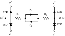 Figure 44. Input Protection Diodes
7.4 Device Functional Modes
7.4.1 Compensating Input Capacitance
The high-input resistance of the LMP7721 allows the use of large feedback and source resistor values without losing gain accuracy due to loading. However, the circuit will be especially sensitive to its layout when these large-value resistors are used.
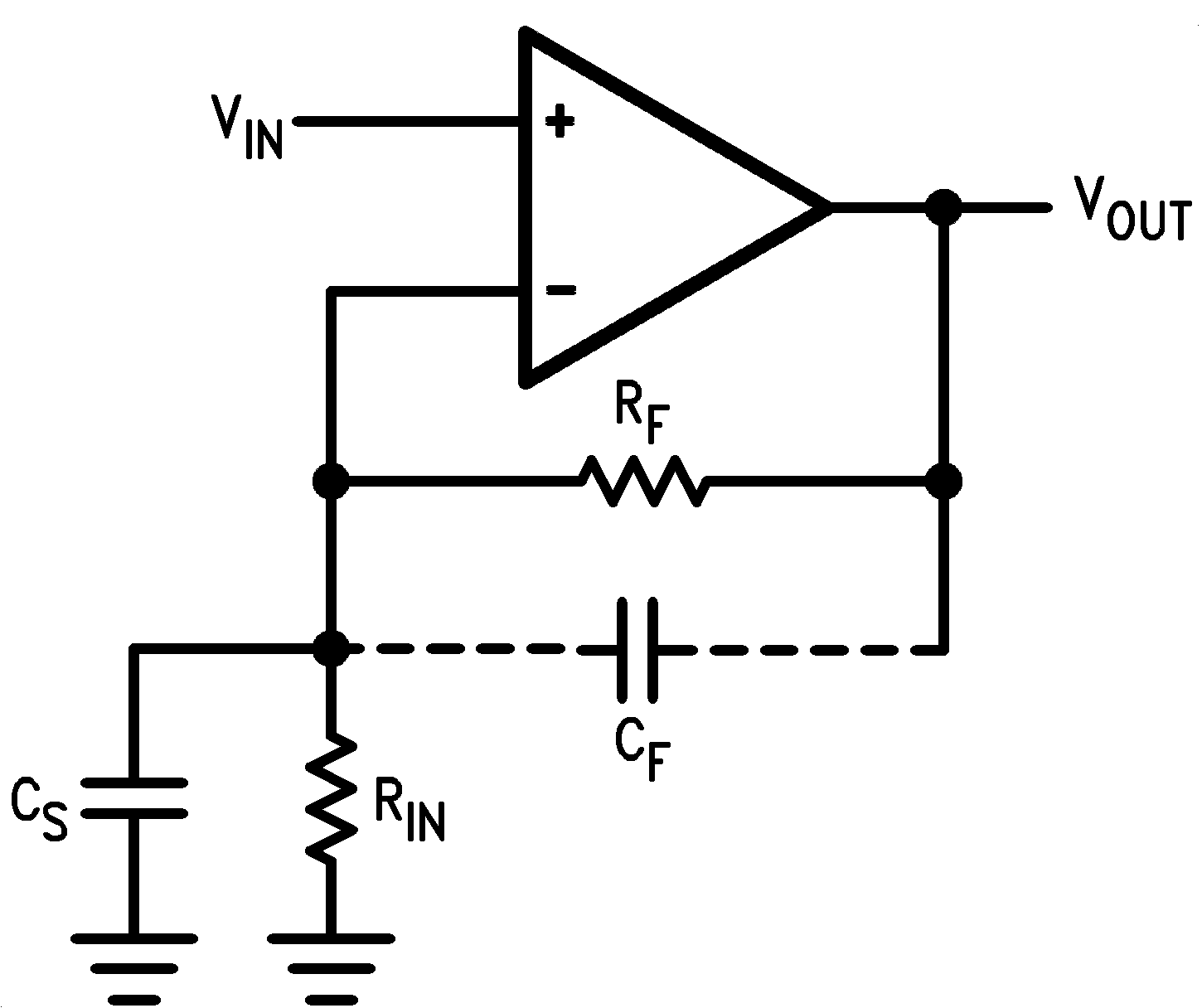 Figure 45. General Operational Amplifier Circuit
Every amplifier has some capacitance between each input and AC ground, and also some differential capacitance between the inputs. When the feedback network around an amplifier is resistive, this input capacitance (along with any additional capacitance due to circuit board traces, the socket, etc.) and the feedback resistors create a pole in the feedback path. This pole can cause gain "peaking" or outright oscillations.
In the General Operational Amplifier circuit, Figure 45 the frequency of this pole is:
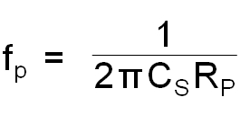
where:
- CS is the total capacitance at the inverting input, including amplifier input capacitance and any stray capacitance from the circuit board traces.
- RP is the parallel combination of RF and RIN
The typical input capacitance of the LMP7721 is about 11pF. This formula, as well as all formulas derived below, apply to inverting and non-inverting op amp configurations.
When the feedback resistors are smaller than a few kΩ, the frequency of the feedback pole will be quite high, since CS is generally less than 15 pF. If the frequency of the feedback pole is much higher than the “ideal” closed-loop bandwidth (the nominal closed-loop bandwidth in the absence of CS), the pole will have a negligible effect on stability, as it will add only a small amount of phase shift.
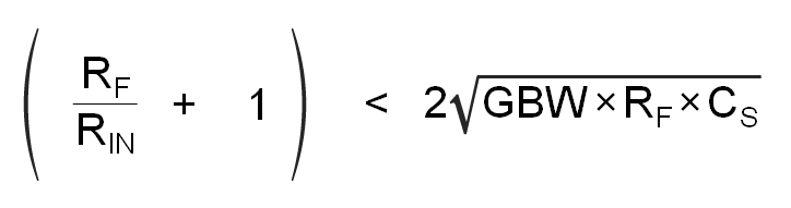
However, if the feedback pole is less than approximately 6 to 10 times the “ideal” −3 dB frequency, a feedback capacitor, CF, should be connected between the output and the inverting input of the op amp. This condition can also be stated in terms of the amplifier’s low-frequency noise gain: To maintain stability a feedback capacitor will probably be needed if
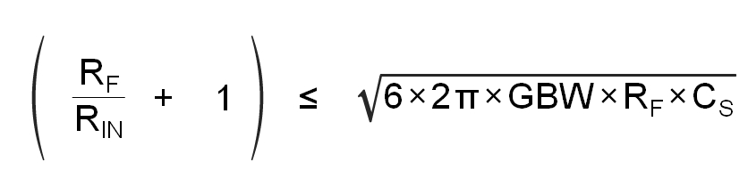
where
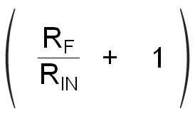
is the amplifier’s low-frequency noise gain and GBW is the amplifier’s gain bandwidth product. An amplifier’s low-frequency noise gain is represented by the formula
regardless of whether the amplifier is being used in inverting or noninverting mode. Note that a feedback capacitor is more likely to be needed when the noise gain is low and/or the feedback resistor is large.
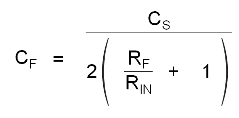
If the above condition is met (indicating a feedback capacitor will probably be needed), and the noise gain is large enough that:
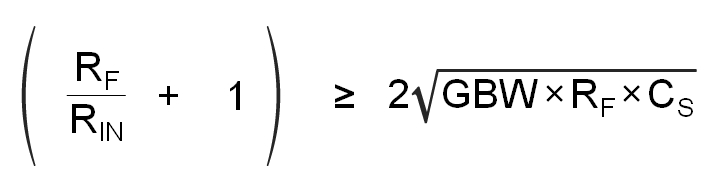
the following value of feedback capacitor is recommended:
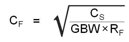
If
the feedback capacitor should be:
Note that these capacitor values are usually significant smaller than those given by the older, more conservative formula:
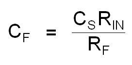
NOTE
CS consists of the amplifier’s input capacitance plus any stray capacitance from the circuit board. CF compensates for the pole caused by CS and the feedback resistors.
Using the smaller capacitors will give much higher bandwidth with little degradation of transient response. It may be necessary in any of the above cases to use a somewhat larger feedback capacitor to allow for unexpected stray capacitance, or to tolerate additional phase shifts in the loop, or excessive capacitive load, or to decrease the noise or bandwidth, or simply because the particular circuit implementation needs more feedback capacitance to be sufficiently stable. For example, a printed circuit board’s stray capacitance may be larger or smaller than the breadboard’s, so the actual optimum value for CF may be different from the one estimated using the breadboard. In most cases, the values of CF should be checked on the actual circuit, starting with the computed value.