SNAS510S January   2011  – January 2016 LMP90097 , LMP90098 , LMP90099 , LMP90100

PRODUCTION DATA.  

  1. Features
  2. Applications
  3. Description
  4. Typical Application Schematic
  5. Revision History
  6. Description (continued)
  7. Pin Configuration and Functions
  8. Specifications
    1. 8.1  Absolute Maximum Ratings
    2. 8.2  ESD Ratings
    3. 8.3  Recommended Operating Conditions
    4. 8.4  Thermal Information
    5. 8.5  Electrical Characteristics
    6. 8.6  SPI Timing Requirements
    7. 8.7  CBS Setup and Hold Timing Requirements
    8. 8.8  SCLK and SDI Timing Requirements
    9. 8.9  SDO Timing Requirements
    10. 8.10 SDO and DRDYB Timing Requirements
    11. 8.11 Typical Characteristics
  9. Detailed Description
    1. 9.1 Overview
    2. 9.2 Functional Block Diagram
    3. 9.3 Feature Description
      1. 9.3.1 True Continuous Background Calibration
      2. 9.3.2 Continuous Background Sensor Diagnostics
      3. 9.3.3 Flexible Input MUX Channels
      4. 9.3.4 Programmable Gain Amplifiers (FGA and PGA)
      5. 9.3.5 Excitation Current Sources (IB1 and IB2) - LMP90100/LMP90098
      6. 9.3.6 Signal Path
        1. 9.3.6.1 Reference Input (VREF)
        2. 9.3.6.2 Flexible Input MUX (VIN)
        3. 9.3.6.3 Selectable Gains (FGA and PGA)
        4. 9.3.6.4 Buffer (BUFF)
        5. 9.3.6.5 Internal/External CLK Selection
        6. 9.3.6.6 Programmable ODRs
        7. 9.3.6.7 Digital Filter
        8. 9.3.6.8 GPIO (D0-D6)
      7. 9.3.7 Calibration
        1. 9.3.7.1 Background Calibration
          1. 9.3.7.1.1 Types of Background Calibration
          2. 9.3.7.1.2 Using Background Calibration
        2. 9.3.7.2 System Calibration
          1. 9.3.7.2.1 System Calibration Offset Coefficient Determination Mode
          2. 9.3.7.2.2 System Calibration Gain Coefficient Determination Mode
          3. 9.3.7.2.3 Post-Calibration Scaling
      8. 9.3.8 Sensor Interface
        1. 9.3.8.1 IB1 and IB2 - Excitation Currents
        2. 9.3.8.2 Burnout Currents
          1. 9.3.8.2.1 Burnout Current Injection
        3. 9.3.8.3 Sensor Diagnostic Flags
          1. 9.3.8.3.1 SHORT_THLD_FLAG
          2. 9.3.8.3.2 RAILS_FLAG
          3. 9.3.8.3.3 POR_AFT_LST_RD:
          4. 9.3.8.3.4 OFLO_FLAGS
          5. 9.3.8.3.5 SAMPLED_CH
      9. 9.3.9 RESET and RESTART
    4. 9.4 Device Functional Modes
      1. 9.4.1 Power Management
      2. 9.4.2 Channels Scan Mode
        1. 9.4.2.1 ScanMode0: Single-Channel Continuous Conversion
        2. 9.4.2.2 ScanMode1: Multiple-Channels Single Scan
        3. 9.4.2.3 ScanMode2: Multiple-Channels Continuous Scan
        4. 9.4.2.4 ScanMode3: Multiple-Channels Continuous Scan with Burnout Currents
    5. 9.5 Programming
      1. 9.5.1  General Rules
      2. 9.5.2  Serial Digital Interface
      3. 9.5.3  Register Address (ADDR)
      4. 9.5.4  Register Read/Write Protocol
      5. 9.5.5  Streaming
      6. 9.5.6  CSB - Chip Select Bar
      7. 9.5.7  SPI Reset
      8. 9.5.8  DRDYB - Data Ready Bar
      9. 9.5.9  DRDYB Case1: Combining SDO/DRDYB with SDO_DRDYB_DRIVER = 0x00
      10. 9.5.10 DRDYB Case2: Combining SDO/DRDYB with SDO_DRDYB_DRIVER = 0x03
      11. 9.5.11 DRDYB Case3: Routing DRDYB to D6
      12. 9.5.12 Data Only Read Transaction
      13. 9.5.13 Cyclic Redundancy Check (CRC)
      14. 9.5.14 Register Read/Write Examples
        1. 9.5.14.1 Writing To Register Examples
        2. 9.5.14.2 Reading From Register Example
      15. 9.5.15 Streaming Examples
        1. 9.5.15.1 Normal Streaming Example
        2. 9.5.15.2 Controlled Streaming Example
    6. 9.6 Register Maps
  10. 10Application and Implementation
    1. 10.1 Application Information
      1. 10.1.1 Quick Start
      2. 10.1.2 ADC_DOUT Calculation
    2. 10.2 Typical Applications
      1. 10.2.1 3-Wire RTD Using 2 Current Sources
        1. 10.2.1.1 Design Requirements
        2. 10.2.1.2 Detailed Design Procedure
        3. 10.2.1.3 Application Curve
      2. 10.2.2 3-Wire RTD Using 1 Current Source
        1. 10.2.2.1 Design Requirements
        2. 10.2.2.2 Detailed Design Procedure
        3. 10.2.2.3 Application Curve
      3. 10.2.3 Thermocouple with Cold Junction Compensation
        1. 10.2.3.1 Design Requirements
        2. 10.2.3.2 Detailed Design Procedure
      4. 10.2.4 Application Curve
  11. 11Power Supply Recommendations
    1. 11.1 VA and VIO
    2. 11.2 VREF
  12. 12Layout
    1. 12.1 Layout Guidelines
    2. 12.2 Layout Example
  13. 13Device and Documentation Support
    1. 13.1 Device Support
      1. 13.1.1 Device Nomenclature
        1. 13.1.1.1 Specific Definitions
    2. 13.2 Related Links
    3. 13.3 Community Resources
    4. 13.4 Trademarks
    5. 13.5 Electrostatic Discharge Caution
    6. 13.6 Glossary
  14. 14Mechanical, Packaging, and Orderable Information

Package Options

Mechanical Data (Package|Pins)
Thermal pad, mechanical data (Package|Pins)
Orderable Information

12 Layout

12.1 Layout Guidelines

  1. Follow the guidelines in the Power Supply Recommendations section.
  2. Keep analog traces away from digital traces.
  3. Never run an analog and digital trace parallel to each other.
  4. If a digital and analog need to cross each other cross them at a 90° angle.
  5. Use a solid ground plane under the LMP90100.
12.2 Layout Example

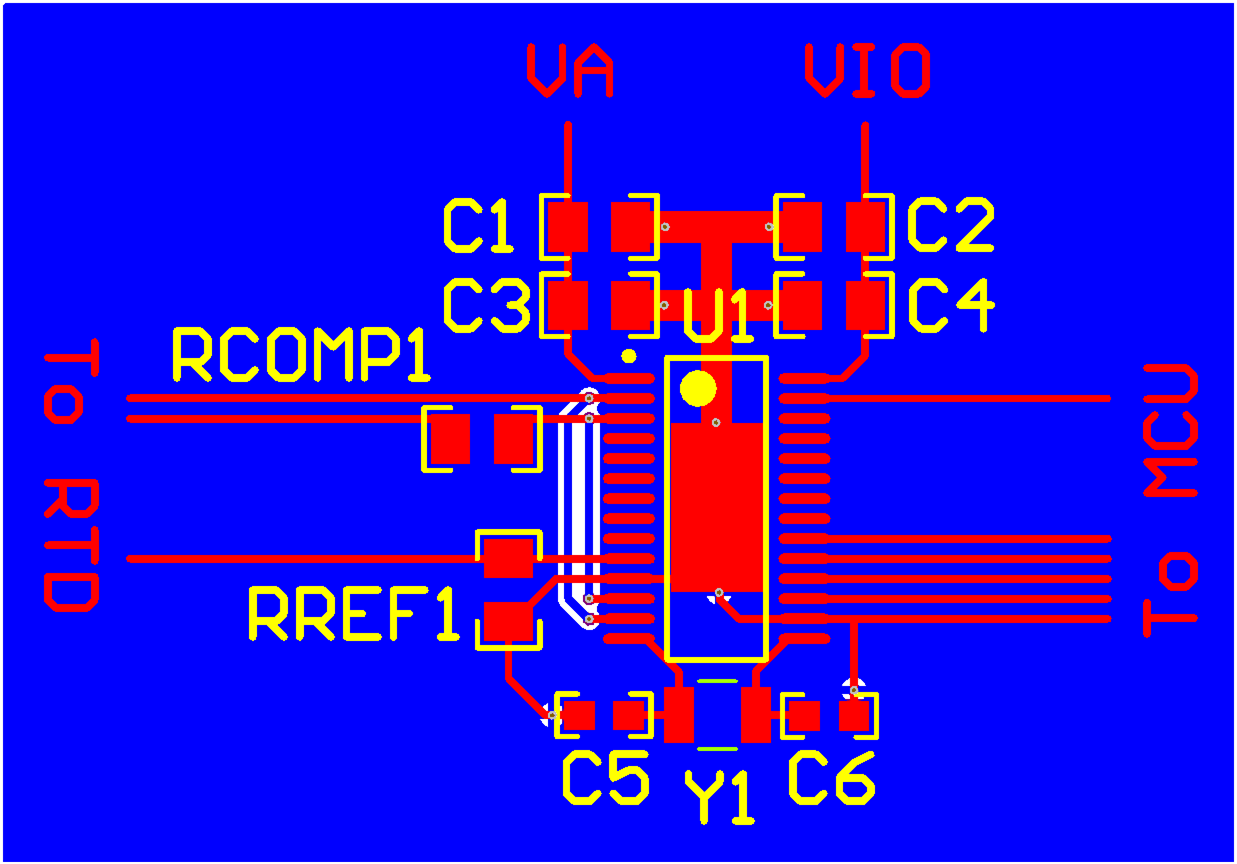
The example layout in Figure 84 is for the Typical Application, 3-Wire RTD Using 2 Current Sources shown in Figure 78.

LMP90100 LMP90099 LMP90098 LMP90097 30169798.gif Figure 84. LMP90xxx Sample Layout