SNAS517E November 2011 – September 2015 LMP91050
PRODUCTION DATA.
- 1 Features
- 2 Applications
- 3 Description
- 4 Revision History
- 5 Description (continued)
- 6 Pin Configuration and Functions
- 7 Specifications
- 8 Detailed Description
- 9 Application and Implementation
- 10Power Supply Recommendations
- 11Layout
- 12Device and Documentation Support
- 13Mechanical, Packaging, and Orderable Information
Package Options
Mechanical Data (Package|Pins)
- DGS|10
Thermal pad, mechanical data (Package|Pins)
Orderable Information
11 Layout
11.1 Layout Guidelines
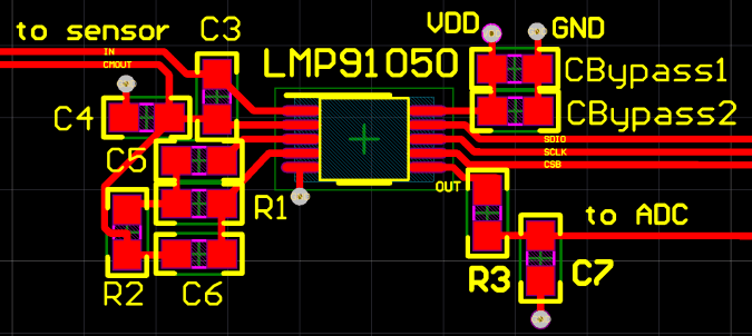
Figure 33 shows a layout example for the LMP91050. All components should be placed as close as possible to the device, especially the bypass capacitors to VDD (CBypass1 and CBypass2).
11.2 Layout Example
 Figure 33. LMP91050 Layout Example