SNVS814B June 2012 – June 2019 LMR10530
PRODUCTION DATA.
- 1 Features
- 2 Applications
- 3 Description
- 4 Revision History
- 5 Pin Configuration and Functions
- 6 Specifications
- 7 Detailed Description
- 8 Application and Implementation
- 9 Layout
- 10Device and Documentation Support
- 11Mechanical, Packaging, and Orderable Information
- 12Mechanical, Packaging, and Orderable Information
Package Options
Mechanical Data (Package|Pins)
- DSC|10
Thermal pad, mechanical data (Package|Pins)
- DSC|10
Orderable Information
7.3.2 Load Step Response
The LMR10530 has a fixed internal loop compensation, which results in a small-signal loop bandwidth highly related to the output voltage level. In general, the loop bandwidth at low voltage is larger than at high voltage due to the increased overall loop gain. The limited bandwidth at high output voltage may pose a challenge when loop step response is concerned. In this case, one effective approach to improving loop step response is to add a feed-forward capacitor CFF) in the range of 27 nF to 100 nF in parallel with the upper feedback resistor (assuming the lower feedback resistor is 2 kΩ), as shown in Figure 21. The feedforward capacitor introduces a zero-pole pair which helps compensate the loop. The position of the zero-pole pair is a function of the feedback resistors and capacitor:


Note the factor in parenthesis is the ratio of the output voltage to the feedback voltage. As the output voltage gets close to 0.6V, the pole moves towards the zero, tending to cancel it out. Consequently, adding CFF will have less effect on the step response at lower output voltages.
As an example, Figure 23 shows that at the output voltage of 3.3 V, 47 nF of CFF can boost the loop bandwidth to 117kHz, from the original 23kHz as shown in Figure 22. Correspondingly, the responses to a load step between 0.3 A and 3 A without and with CFF are shown in Figure 24 and Figure 25 respectively. The higher loop bandwidth as a result of CFF reduces the total output excursion by more than half.
Aside from the above approach, increasing the output capacitance is generally also effective to reduce the excursion in output voltage caused by a load step. This approach remains valid for applications where the desired output voltages are close to the feedback voltage.
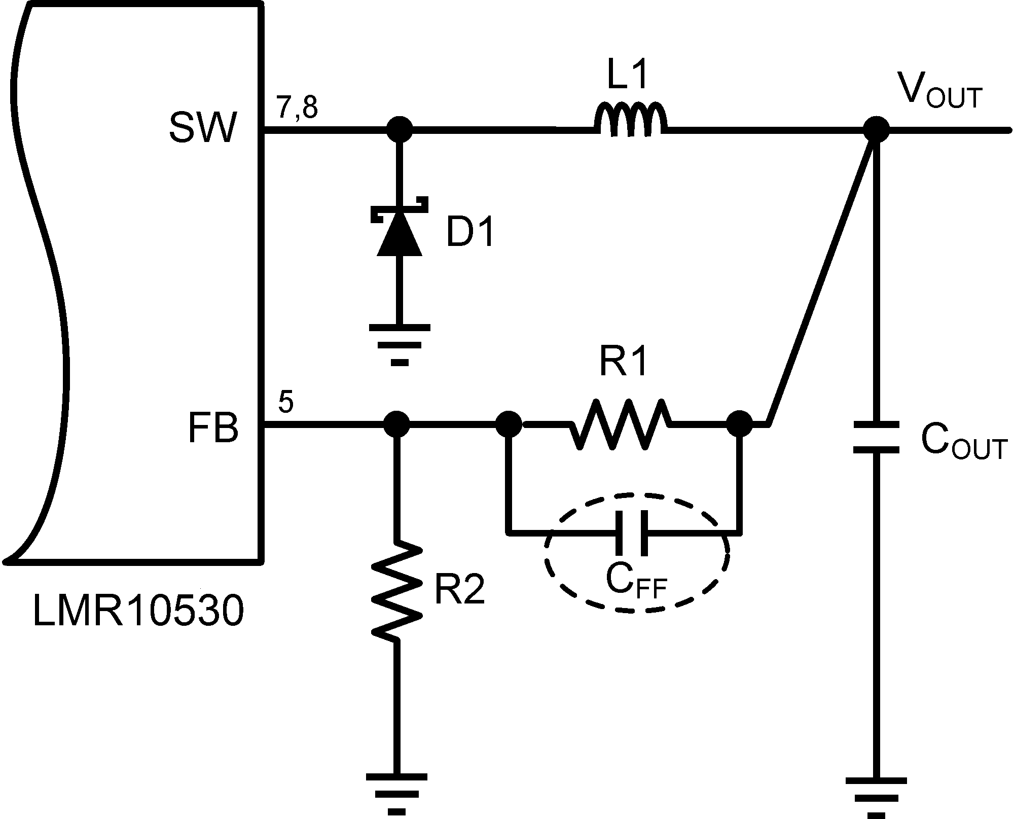 Figure 21. Adding a CFF Capacitor
 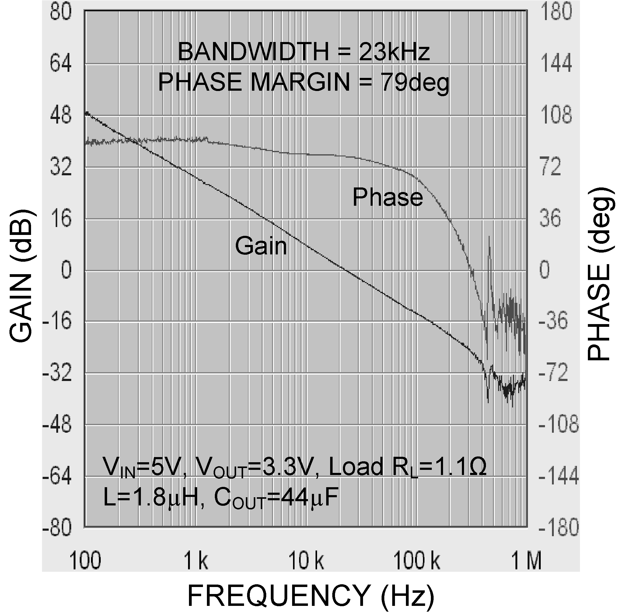 Figure 22. Loop Gain and Phase Without CFF
 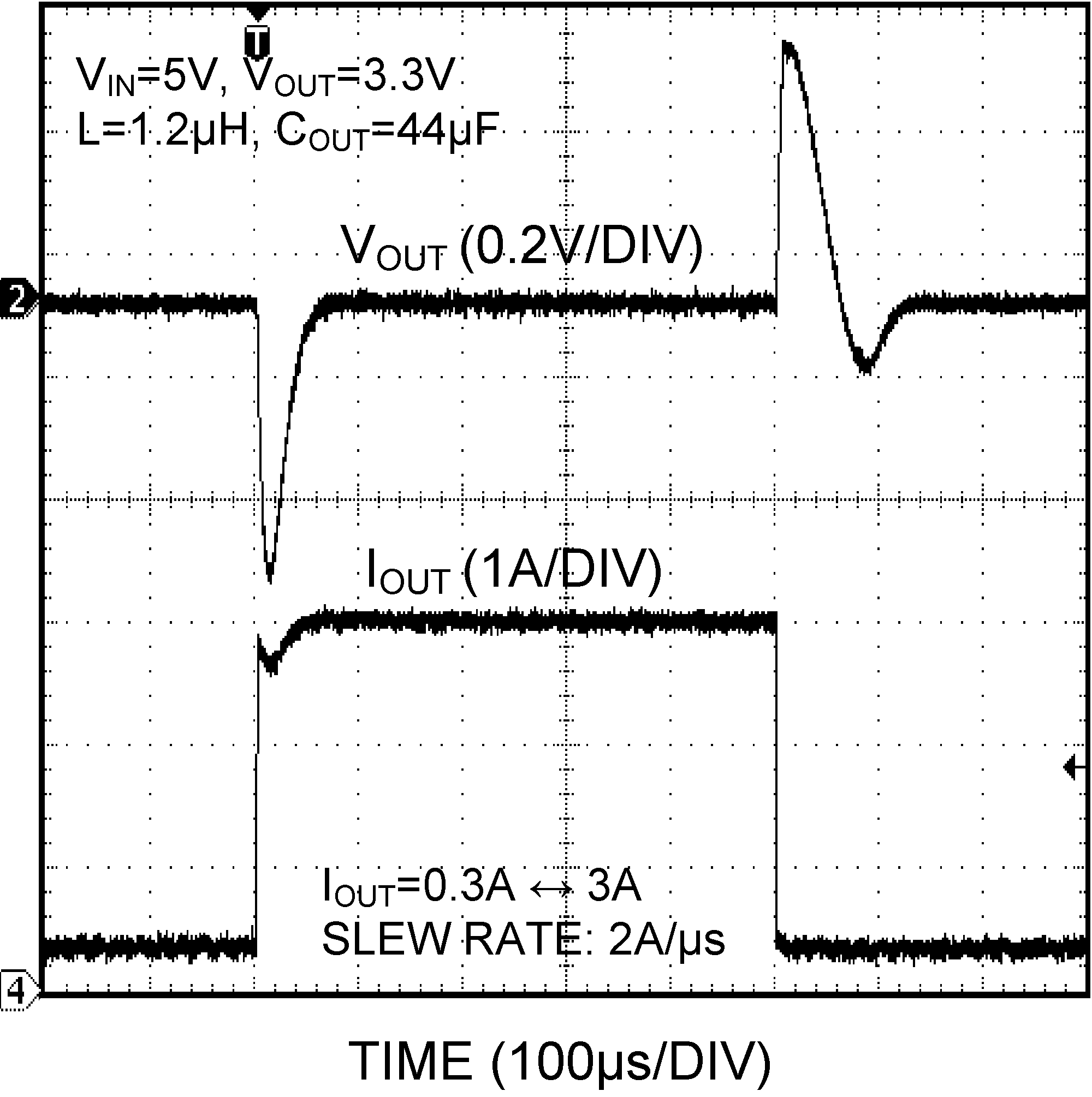 Figure 24. Load Step Response Without CFF
 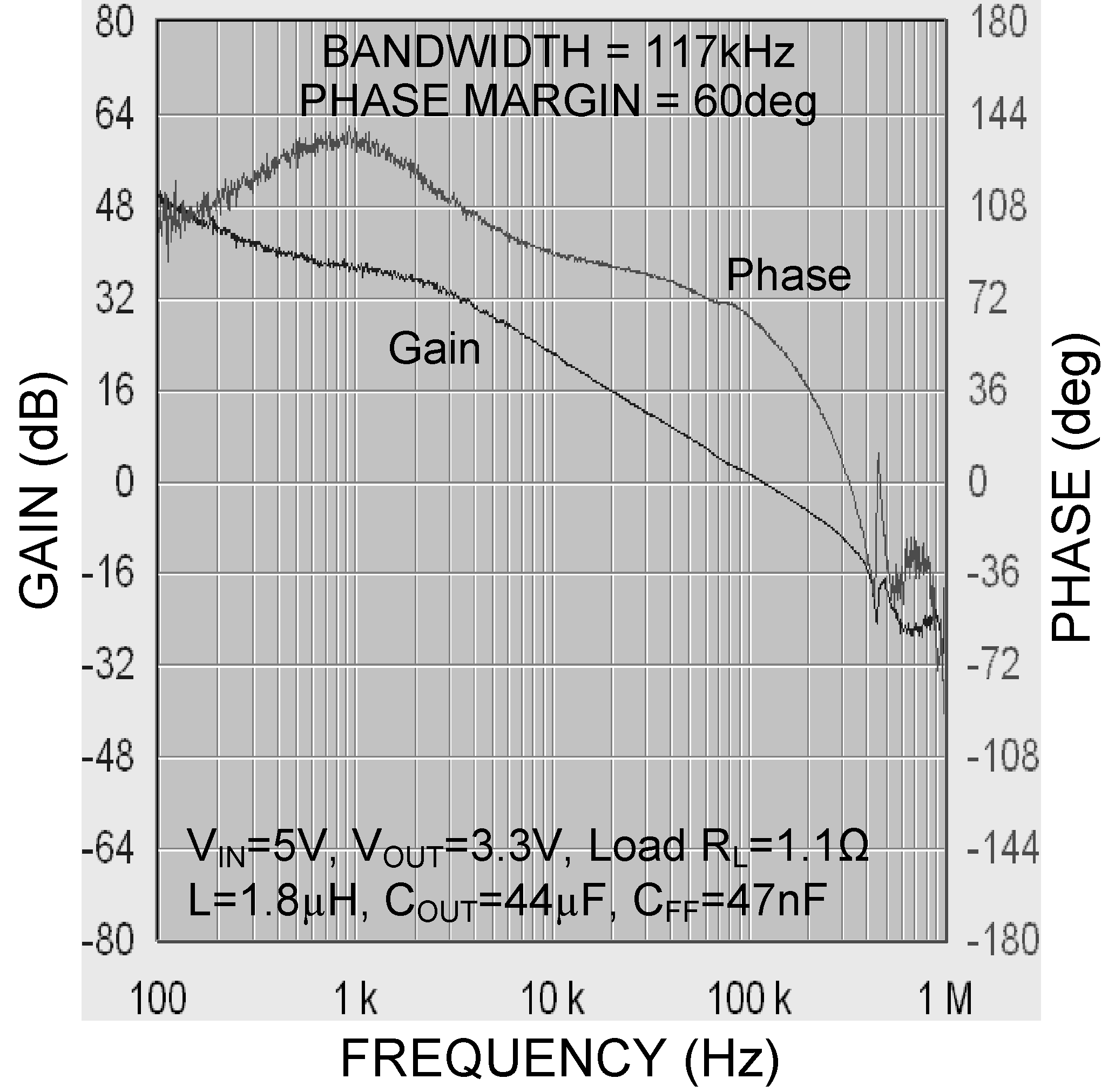 Figure 23. Loop Gain and Phase With CFF
 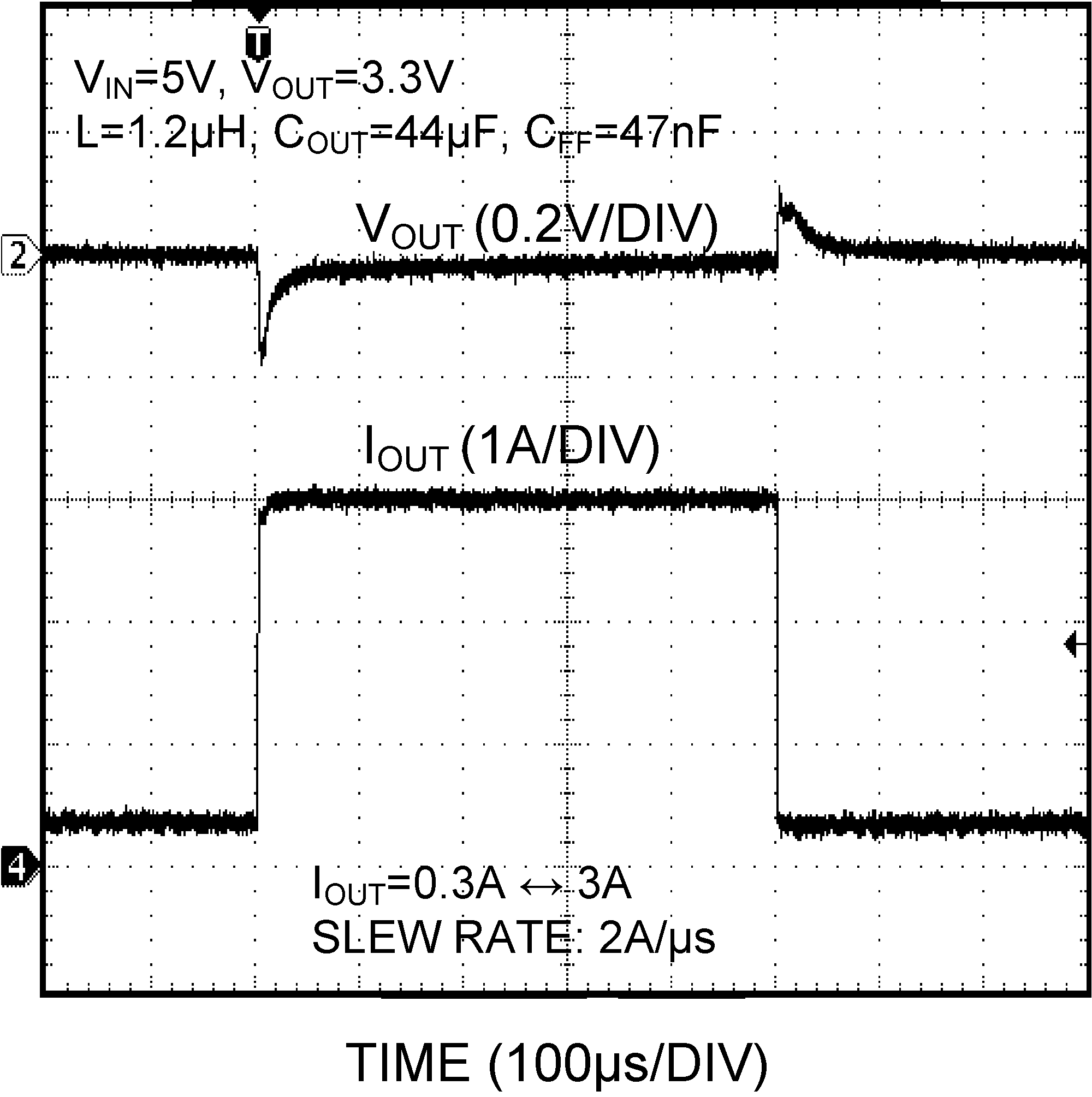 Figure 25. Load Step Response With CFF